


Request Quote
(Ships tomorrow)
LF412ACN/NOPB Equivalent & Substitute Parts
Part Overview
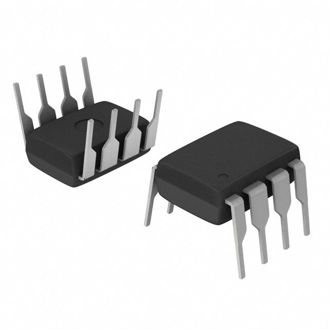
The LF412ACN/NOPB is a J-FET input operational amplifier manufactured by Texas Instruments, configured as a dual-channel (2 circuit) device in an 8-DIP through-hole package. This component is classified as a linear amplifier and maintains Active product status with ROHS3 compliance. The LF412ACN/NOPB is specified for general-purpose J-FET amplifier applications requiring low input bias current and moderate bandwidth performance across industrial and commercial temperature ranges (0°C to 70°C). Equivalent and substitute parts are identified based on matching electrical parameters, package configuration, and functional compatibility within the J-FET operational amplifier category.
Substiute Parts
Key Parameters
| Parameter | LF412ACN/NOPB Value | Unit | Substitution Relevance |
|---|---|---|---|
| Amplifier Type | J-FET | — | Critical: Defines input stage architecture |
| Number of Circuits | 2 | Channels | Critical: Functional configuration |
| Package / Case | 8-DIP (0.300", 7.62mm) | — | Critical: Physical and electrical compatibility |
| Slew Rate | 15 | V/µs | Important: Dynamic response capability |
| Gain Bandwidth Product | 4 | MHz | Important: Frequency response envelope |
| Current - Input Bias | 50 | pA | Important: Input loading characteristics |
| Voltage - Input Offset | 500 | µV | Important: DC accuracy specification |
| Current - Supply | 3.6 (x2 Channels) | mA | Important: Power consumption per channel |
| Voltage - Supply Span (Min) | 10 | V | Critical: Minimum operating voltage |
| Voltage - Supply Span (Max) | 44 | V | Critical: Maximum operating voltage |
| Operating Temperature | 0 to 70 | °C | Important: Temperature rating class |
| Mounting Type | Through Hole | — | Critical: PCB assembly compatibility |
| RoHS Status | ROHS3 Compliant | — | Important: Environmental compliance |
Substitute Part Grouping Explanation
Substitute parts for the LF412ACN/NOPB are identified based on strict alignment with the following critical and important parameters:
Critical Parameters (Must Match):
- Amplifier Type: J-FET input configuration
- Number of Circuits: Dual-channel (2 circuit) topology
- Package / Case: 8-DIP (0.300", 7.62mm) through-hole form factor
- Voltage - Supply Span: Operating range must encompass or be compatible with 10V minimum and 44V maximum
- Mounting Type: Through-hole technology
Important Parameters (Determine Functional Equivalence):
- Slew Rate: 15V/µs baseline; substitutes within ±50% acceptable for most applications
- Gain Bandwidth Product: 4 MHz baseline; substitutes within ±50% acceptable
- Current - Input Bias: 50 pA baseline; lower values acceptable, higher values require application review
- Voltage - Input Offset: 500 µV baseline; lower values acceptable
- Current - Supply: 3.6 mA per channel baseline; lower values preferred for power-sensitive applications
- Operating Temperature: 0°C to 70°C; extended range acceptable
- RoHS Status: ROHS3 compliance required for regulatory alignment
Substitutes are grouped into three categories based on performance characteristics relative to the LF412ACN/NOPB baseline.
Parameter Comparison
| Part Number | Manufacturer | Slew Rate (V/µs) | GBW (MHz) | Input Bias (pA) | Input Offset (µV) | Supply Current (mA) | Supply Min (V) | Supply Max (V) | Temp Range (°C) | RoHS |
|---|---|---|---|---|---|---|---|---|---|---|
| LF412ACN/NOPB | Texas Instruments | 15 | 4 | 50 | 500 | 3.6 | 10 | 44 | 0 to 70 | ROHS3 |
| LF412CN/NOPB | Texas Instruments | 15 | 4 | 50 | 1000 | 3.6 | 10 | 40 | 0 to 70 | ROHS3 |
| LF412CP | Texas Instruments | 13 | 3 | 50 | 500 | 4.5 | 7 | 36 | 0 to 70 | ROHS3 |
| AD648JNZ | Analog Devices Inc. | 1.8 | 1 | 5 | 750 | 0.34 | 9 | 36 | 0 to 70 | ROHS3 |
| AD648KNZ | Analog Devices Inc. | 1.8 | 1 | 3 | 300 | 0.34 | 9 | 36 | 0 to 70 | ROHS3 |
| AD712KNZ | Analog Devices Inc. | 20 | 4 | 25 | 300 | 5 | 9 | 36 | 0 to 70 | ROHS3 |
| AD746JNZ | Analog Devices Inc. | 75 | 13 | 110 | 300 | 7 | 9 | 36 | 0 to 70 | ROHS3 |
| LT1057ACN8#PBF | Analog Devices Inc. | 14 | 5 | 5 | 150 | 1.6 | 20 | 36 | 0 to 70 | ROHS3 |
| LT1057CN8#PBF | Analog Devices Inc. | 13 | 5 | 7 | 200 | 1.7 | 20 | 36 | 0 to 70 | ROHS3 |
| LT1113ACN8#PBF | Analog Devices Inc. | 3.9 | 5.6 | 300 | 450 | 5.3 | 9 | 40 | -40 to 85 | ROHS3 |
| LT1113CN8#PBF | Analog Devices Inc. | 3.9 | 5.6 | 300 | 550 | 5.3 | 9 | 40 | -40 to 85 | ROHS3 |
Engineering Selection Recommendations
Tier 1: Direct Substitutes (Highest Compatibility)
LF412CN/NOPB and LF412CP are Texas Instruments products within the LF412 base product family. Both maintain the same amplifier type (J-FET), circuit count (2), and package configuration (8-DIP through-hole). LF412CN/NOPB differs only in input offset voltage specification (1 mV vs. 500 µV) and maximum supply voltage (40V vs. 44V). LF412CP exhibits reduced slew rate (13V/µs vs. 15V/µs), reduced gain-bandwidth product (3 MHz vs. 4 MHz), and increased supply current (4.5 mA vs. 3.6 mA), with a lower minimum supply voltage (7V vs. 10V). Both maintain ROHS3 compliance and Active product status. Selection between these variants depends on specific application requirements for offset voltage tolerance and supply voltage range.
Tier 2: Functional Equivalents with Performance Trade-offs
AD712KNZ (Analog Devices Inc.) provides superior slew rate (20V/µs) and maintains 4 MHz gain-bandwidth product with lower input bias current (25 pA). Supply voltage range is reduced (9V to 36V). This substitute is suitable for applications requiring faster transient response within the constrained supply range.
LT1057ACN8#PBF and LT1057CN8#PBF (Analog Devices Inc., LT® series) offer slew rates (14V/µs and 13V/µs respectively) and gain-bandwidth products (5 MHz) comparable to or exceeding the baseline. Input bias current is significantly lower (5 pA and 7 pA). Supply current is reduced (1.6 mA and 1.7 mA per channel). However, minimum supply voltage is elevated to 20V, restricting use in lower-voltage applications. These substitutes are optimal for low-power, higher-voltage system designs.
Tier 3: Specialized Alternatives
AD648JNZ and AD648KNZ (Analog Devices Inc.) feature extremely low supply current (340 µA per channel) and low input bias current (5 pA and 3 pA respectively). Slew rate and gain-bandwidth product are significantly reduced (1.8V/µs and 1 MHz). These substitutes are applicable only to applications where bandwidth and slew rate constraints are acceptable in exchange for ultra-low power consumption.
AD746JNZ (Analog Devices Inc.) provides the highest performance envelope with 75V/µs slew rate and 13 MHz gain-bandwidth product. Input bias current is elevated (110 pA). Supply current is increased (7 mA). This substitute is suitable for high-speed, high-bandwidth applications where the LF412ACN/NOPB baseline performance is insufficient.
LT1113ACN8#PBF and LT1113CN8#PBF (Analog Devices Inc., LT® series) extend operating temperature range to -40°C to 85°C. Slew rate is reduced (3.9V/µs) and input bias current is elevated (300 pA). These substitutes are applicable to extended-temperature industrial and automotive environments.
Compliance and Regulatory Alignment
All listed substitutes maintain ROHS3 compliance and Active product status, ensuring regulatory alignment with the original LF412ACN/NOPB specification. Moisture sensitivity level (MSL) is uniformly rated at 1 (Unlimited) across all substitutes, indicating no special handling requirements during storage or assembly.
Frequently Asked Questions (FAQ)
Q1: Can LF412CN/NOPB directly replace LF412ACN/NOPB in all applications?
LF412CN/NOPB is a direct substitute within the same product family with identical slew rate (15V/µs) and gain-bandwidth product (4 MHz). The primary difference is input offset voltage specification (1 mV vs. 500 µV) and maximum supply voltage (40V vs. 44V). If your application operates below 40V and can tolerate 1 mV input offset, LF412CN/NOPB is a compatible substitute. If your design requires the 44V maximum supply voltage or 500 µV offset specification, verify compatibility before substitution.
Q2: What is the key difference between Texas Instruments LF412 variants and Analog Devices alternatives?
Texas Instruments LF412 variants (LF412ACN/NOPB, LF412CN/NOPB, LF412CP) are within the same product line with consistent J-FET architecture and 8-DIP packaging. Analog Devices alternatives (AD648, AD712, AD746, LT1057, LT1113 series) offer different performance envelopes. AD712KNZ and AD746JNZ provide higher slew rates and bandwidth. LT1057 series offers lower supply current. AD648 series prioritizes ultra-low power consumption. Selection depends on whether your application prioritizes speed, power efficiency, or other performance metrics.
Q3: Can I use AD746JNZ as a drop-in replacement for LF412ACN/NOPB?
AD746JNZ is physically compatible (8-DIP through-hole package) and functionally compatible (J-FET dual-channel amplifier). However, AD746JNZ exhibits significantly higher performance specifications: 75V/µs slew rate (vs. 15V/µs), 13 MHz gain-bandwidth product (vs. 4 MHz), and 110 pA input bias current (vs. 50 pA). In applications designed for LF412ACN/NOPB performance, AD746JNZ will operate correctly but may introduce unexpected behavior due to higher bandwidth and faster transient response. Verify circuit stability and signal integrity before substitution in precision analog applications.
Q4: Which substitute offers the lowest power consumption?
AD648JNZ and AD648KNZ offer the lowest supply current at 340 µA per channel (vs. 3.6 mA for LF412ACN/NOPB). However, these devices sacrifice significant performance: slew rate is 1.8V/µs (vs. 15V/µs) and gain-bandwidth product is 1 MHz (vs. 4 MHz). Selection of AD648 series is appropriate only for battery-powered or energy-constrained applications where bandwidth limitations are acceptable.
Q5: Are all substitutes rated for the same temperature range as LF412ACN/NOPB?
LF412ACN/NOPB is rated 0°C to 70°C. Most substitutes (LF412CN/NOPB, LF412CP, AD648JNZ, AD648KNZ, AD712KNZ, AD746JNZ, LT1057ACN8#PBF, LT1057CN8#PBF) maintain this same range. LT1113ACN8#PBF and LT1113CN8#PBF extend the range to -40°C to 85°C for industrial and automotive applications. If your application requires extended temperature operation, LT1113 series is the appropriate selection.
Q6: What is the significance of the 8-DIP package specification?
The 8-DIP (0.300", 7.62mm) package is a through-hole dual inline package with 0.3-inch row spacing and 7.62 mm lead pitch. All listed substitutes use identical packaging, ensuring mechanical and electrical compatibility on PCBs designed for the LF412ACN/NOPB. Pin-to-pin compatibility is guaranteed across all substitutes listed in this reference.
Q7: Do all substitutes meet ROHS3 compliance?
Yes. All substitutes listed in this reference maintain ROHS3 compliance status, matching the environmental and regulatory requirements of the LF412ACN/NOPB. Moisture sensitivity level (MSL) is uniformly rated at 1 (Unlimited), indicating no special handling or storage requirements.
Q8: Which substitute is best for high-speed signal conditioning applications?
AD746JNZ provides the highest performance envelope with 75V/µs slew rate and 13 MHz gain-bandwidth product, making it suitable for high-speed applications. If your design requires faster transient response than LF412ACN/NOPB but does not require maximum performance, AD712KNZ offers a balanced alternative with 20V/µs slew rate and 4 MHz bandwidth at lower supply current than AD746JNZ.
Q9: Can I substitute LT1057ACN8#PBF in a circuit designed for ±15V dual supply operation?
LT1057ACN8#PBF requires a minimum supply voltage of 20V (vs. 10V for LF412ACN/NOPB). In a ±15V dual supply configuration (±15V = 30V total), LT1057ACN8#PBF operates within specification. However, verify that your circuit design does not rely on the lower minimum supply voltage of the original LF412ACN/NOPB. If your design operates at lower supply voltages, LT1057ACN8#PBF is not compatible.
Q10: What is the practical difference between LT1113ACN8#PBF and LT1113CN8#PBF?
Both devices are identical except for input offset voltage specification: LT1113ACN8#PBF is specified at 450 µV, while LT1113CN8#PBF is specified at 550 µV. Both extend operating temperature to -40°C to 85°C. Selection between these variants depends on DC accuracy requirements. For applications requiring tighter offset voltage tolerance, LT1113ACN8#PBF is the appropriate choice.
Alternative Parts

SJ6012L2TP
Littelfuse Inc.
6 Alternative Parts

JMK107BBJ476MA-RE
Taiyo Yuden
10 Alternative Parts

GMK107BBJ475MA-T
Taiyo Yuden
5 Alternative Parts
SJ6020N2ARP
Littelfuse Inc.
3 Alternative Parts
SJ6025R2ATP
Littelfuse Inc.
4 Alternative Parts

2474-05L
API Delevan Inc.
1 Alternative Parts

4590R-684K
API Delevan Inc.
1 Alternative Parts

CM6560R-334
API Delevan Inc.
1 Alternative Parts

CM6460-104
API Delevan Inc.
1 Alternative Parts

5526-12
API Delevan Inc.
1 Alternative Parts