


Request Quote
(Ships tomorrow)
JS28F128P30TF75A Equivalent & Substitute Parts
Part Overview
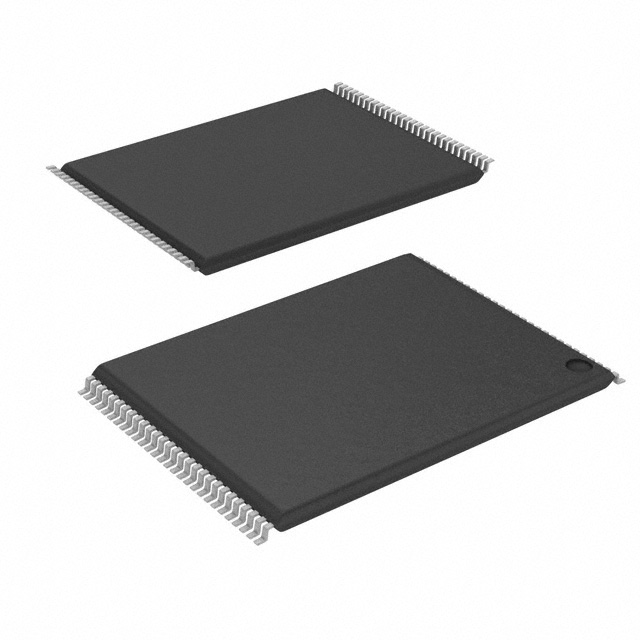
The JS28F128P30TF75A is a 128Mbit NOR Flash memory IC manufactured by Micron Technology Inc., featuring parallel interface architecture in a 56-TSOP surface mount package. This component is classified as obsolete, necessitating identification of functionally equivalent alternatives for ongoing system support and new design implementations. The part operates within a 1.7V to 2V supply range with 75 ns access time and 40 MHz clock frequency capability.
Substiute Parts
Key Parameters
| Parameter | Value |
|---|---|
| Memory Size | 128Mbit |
| Memory Format | FLASH |
| Technology | FLASH - NOR |
| Memory Organization | 8M x 16 |
| Memory Interface | Parallel |
| Package / Case | 56-TFSOP (0.724", 18.40mm Width) |
| Mounting Type | Surface Mount |
| Access Time | 75 ns |
| Clock Frequency | 40 MHz |
| Voltage - Supply | 1.7V ~ 2V |
| Operating Temperature | -40°C ~ 85°C (TA) |
| RoHS Status | ROHS3 Compliant |
| Moisture Sensitivity Level (MSL) | 3 (168 Hours) |
Substitute Part Grouping Explanation
Substitution eligibility for the JS28F128P30TF75A is determined by the following critical parameters:
- Memory capacity: 128Mbit minimum requirement
- Memory technology: FLASH - NOR architecture
- Memory interface: Parallel interface configuration
- Package compatibility: 56-TSOP surface mount form factor
- Operating temperature range: -40°C to 85°C minimum coverage
- RoHS compliance: ROHS3 Compliant status
The MT28EW128ABA1HJS-0SIT meets these core substitution criteria. Both components share identical memory capacity, NOR Flash technology, parallel interface architecture, and 56-TSOP packaging. Both maintain ROHS3 compliance and identical operating temperature specifications. Differences in access time (95 ns vs. 75 ns), clock frequency capability, and supply voltage range represent performance and operational variations that must be evaluated within specific application contexts.
Parameter Comparison
| Parameter | JS28F128P30TF75A | MT28EW128ABA1HJS-0SIT |
|---|---|---|
| Manufacturer | Micron Technology Inc. | Micron Technology Inc. |
| Memory Size | 128Mbit | 128Mbit |
| Memory Format | FLASH | FLASH |
| Technology | FLASH - NOR | FLASH - NOR |
| Memory Organization | 8M x 16 | 16M x 8, 8M x 16 |
| Memory Interface | Parallel | Parallel |
| Package / Case | 56-TFSOP (0.724", 18.40mm Width) | 56-TFSOP (0.724", 18.40mm Width) |
| Mounting Type | Surface Mount | Surface Mount |
| Access Time | 75 ns | 95 ns |
| Clock Frequency | 40 MHz | Not specified |
| Write Cycle Time - Word, Page | 75 ns | 60 ns |
| Voltage - Supply | 1.7V ~ 2V | 2.7V ~ 3.6V |
| Operating Temperature | -40°C ~ 85°C (TA) | -40°C ~ 85°C (TA) |
| Product Status | Obsolete | Active |
| RoHS Status | ROHS3 Compliant | ROHS3 Compliant |
| Moisture Sensitivity Level (MSL) | 3 (168 Hours) | 3 (168 Hours) |
Engineering Selection Recommendations
The MT28EW128ABA1HJS-0SIT represents the primary active substitute for the obsolete JS28F128P30TF75A. Both components maintain identical ROHS3 compliance certification and REACH unaffected status, ensuring regulatory alignment. The substitute part carries active product status with significantly higher inventory availability (18005 Pcs vs. 1752 Pcs), supporting long-term supply chain continuity.
Critical design consideration: The supply voltage differential between the two components (1.7V-2V vs. 2.7V-3.6V) requires circuit-level evaluation. Applications designed for the original part's lower voltage specification cannot directly substitute the MT28EW128ABA1HJS-0SIT without power supply architecture modification. Conversely, systems operating at 2.7V-3.6V can accommodate the substitute without voltage-related constraints.
Access time specification (95 ns vs. 75 ns) and write cycle time (60 ns vs. 75 ns) represent performance characteristics that must align with system timing requirements. The substitute part's longer access time may impact applications with strict timing constraints.
Frequently Asked Questions (FAQ)
Q: Can the MT28EW128ABA1HJS-0SIT directly replace the JS28F128P30TF75A in existing designs?
A: Direct replacement requires verification of two critical factors: supply voltage compatibility and timing margin availability. The substitute operates at 2.7V-3.6V versus the original's 1.7V-2V specification. If your system power supply cannot accommodate this voltage range, circuit modification is necessary. Additionally, the substitute's 95 ns access time versus the original's 75 ns must not violate system timing requirements.
Q: Are both parts physically compatible in the same PCB footprint?
A: Yes. Both components utilize identical 56-TFSOP packaging with 0.724" (18.40mm) width specification, ensuring mechanical and electrical footprint compatibility at the board level.
Q: What is the significance of the memory organization difference (8M x 16 vs. 16M x 8, 8M x 16)?
A: The substitute part supports dual memory organization modes, including the original's 8M x 16 configuration. This flexibility ensures address and data bus compatibility for applications designed around the original part's organization scheme.
Q: Why is the substitute part's write cycle time faster (60 ns vs. 75 ns) despite longer access time?
A: Write cycle time and access time measure different operational parameters. Access time defines read operation latency, while write cycle time specifies the duration required to complete a write operation. These parameters are independently specified and do not correlate directly.
Q: Are there compliance or certification differences between the two parts?
A: Both components maintain identical ROHS3 compliance, REACH unaffected status, and MSL 3 (168 Hours) moisture sensitivity classification. No compliance differentiation exists between the parts.
Alternative Parts

SJ6012L2TP
Littelfuse Inc.
6 Alternative Parts

JMK107BBJ476MA-RE
Taiyo Yuden
10 Alternative Parts

GMK107BBJ475MA-T
Taiyo Yuden
5 Alternative Parts
SJ6020N2ARP
Littelfuse Inc.
3 Alternative Parts
SJ6025R2ATP
Littelfuse Inc.
4 Alternative Parts

2474-05L
API Delevan Inc.
1 Alternative Parts

4590R-684K
API Delevan Inc.
1 Alternative Parts

CM6560R-334
API Delevan Inc.
1 Alternative Parts

CM6460-104
API Delevan Inc.
1 Alternative Parts

5526-12
API Delevan Inc.
1 Alternative Parts