


Request Quote
(Ships tomorrow)
IXTP8N50P N-Channel 500V 8A MOSFET Equivalent & Substitute Parts
Part Overview
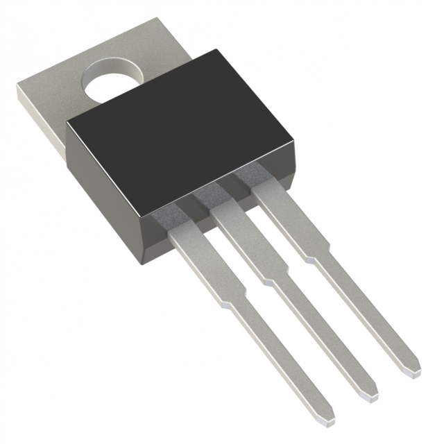
The IXTP8N50P is an N-Channel 500V 8A MOSFET manufactured by IXYS in the PolarHV™ series, housed in a TO-220-3 through-hole package. This device is rated for 150W power dissipation and operates across a temperature range of -55°C to 150°C. The part is currently obsolete, necessitating identification of functionally equivalent alternatives for ongoing system support and new designs requiring similar electrical characteristics.
Substiute Parts
Key Parameters
| Parameter | Value | Unit |
|---|---|---|
| FET Type | N-Channel | — |
| Drain to Source Voltage (Vdss) | 500 | V |
| Continuous Drain Current (Id) @ 25°C | 8 | A |
| Power Dissipation (Max) | 150 | W |
| Rds On (Max) @ 4A, 10V | 800 | mOhm |
| Gate Threshold Voltage (Vgs(th)) @ 100µA | 5.5 | V |
| Gate Charge (Qg) @ 10V | 20 | nC |
| Operating Temperature Range | -55 to 150 | °C |
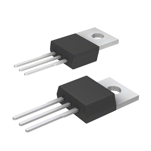
| Package Type | TO-220-3 | — |
| Mounting Type | Through Hole | — |
Substitute Part Grouping Explanation
Substitution of the IXTP8N50P is determined by the following critical parameters:
Primary Substitution Criteria:
- Drain to Source Voltage (Vdss): 500V minimum
- Continuous Drain Current (Id): 8A or greater
- Package Type: TO-220-3 through-hole configuration
- Operating Temperature Range: -55°C to 150°C
- Power Dissipation: 150W or greater
Secondary Compatibility Factors:
- Gate Threshold Voltage (Vgs(th)): 4V to 5.5V range
- Maximum Gate Charge (Qg): 20nC to 40nC range
- Rds On (Max): 500mOhm to 850mOhm range
- Gate Voltage (Vgs Max): ±30V
Substitute parts must maintain electrical compatibility within these parameter boundaries to ensure functional equivalence in circuit applications. Parts with higher voltage ratings or current capabilities operate as direct substitutes when other parameters remain within acceptable ranges.
Parameter Comparison
| Parameter | IXTP8N50P | IXTP8N65X2 | AOT9N50 | IRF840APBF | IRF840LCPBF | STP8NM50N | STP9NK50Z |
|---|---|---|---|---|---|---|---|
| Manufacturer | IXYS | IXYS | Alpha & Omega | Vishay Siliconix | Vishay Siliconix | STMicroelectronics | STMicroelectronics |
| Vdss (V) | 500 | 650 | 500 | 500 | 500 | 500 | 500 |
| Id @ 25°C (A) | 8 | 8 | 9 | 8 | 8 | 5 | 7.2 |
| Power Dissipation (W) | 150 | 150 | 192 | 125 | 125 | 45 | 110 |
| Rds On @ 10V (mOhm) | 800 | 500 | 850 | 850 | 850 | 790 | 850 |
| Vgs(th) (V) | 5.5 | 5 | 4.5 | 4 | 4 | 4 | 4.5 |
| Gate Charge Qg (nC) | 20 | 12 | 28 | 38 | 39 | 14 | 32 |
| Vgs Max (V) | ±30 | ±30 | ±30 | ±30 | ±30 | ±25 | ±30 |
| Operating Temp Range (°C) | -55 to 150 | -55 to 150 | -55 to 150 | -55 to 150 | -55 to 150 | 0 to 150 | -55 to 150 |
| Package | TO-220-3 | TO-220-3 | TO-220-3 | TO-220-3 | TO-220-3 | TO-220-3 | TO-220-3 |
| Product Status | Obsolete | Active | Not For New Designs | Active | Active | Active | Active |
| RoHS Status | Not Specified | ROHS3 Compliant | ROHS3 Compliant | ROHS3 Compliant | ROHS3 Compliant | ROHS3 Compliant | ROHS3 Compliant |
Engineering Selection Recommendations
Tier 1 Substitutes (Direct Equivalents):
IRF840LCPBF and IRF840APBF (Vishay Siliconix) are the primary recommended substitutes. Both devices match the IXTP8N50P across all critical electrical parameters: 500V Vdss, 8A continuous drain current, TO-220-3 package, and -55°C to 150°C operating range. Both are active products with ROHS3 compliance. IRF840LCPBF offers superior inventory availability (23,636 units) and REACH Unaffected status. IRF840APBF provides REACH Affected designation but maintains active production status.
Tier 2 Substitutes (Enhanced Performance):
IXTP8N65X2 (IXYS, Ultra X2 series) provides higher voltage rating (650V Vdss) while maintaining 8A current and 150W power dissipation. This device offers improved Rds On performance (500mOhm vs. 800mOhm) and lower gate charge (12nC vs. 20nC), resulting in reduced switching losses. Active product status with ROHS3 compliance. Suitable for applications requiring enhanced voltage margin.
AOT9N50 (Alpha & Omega Semiconductor) delivers higher current capability (9A vs. 8A) and increased power dissipation (192W vs. 150W) at identical 500V Vdss. Gate charge is elevated (28nC), indicating higher switching losses. Product status is "Not For New Designs," limiting suitability for new development.
Tier 3 Substitutes (Reduced Performance):
STP9NK50Z (STMicroelectronics, SuperMESH™ series) provides 7.2A continuous current and 110W power dissipation at 500V Vdss. This device operates within acceptable parameter ranges but with reduced current and power handling. Active product with ROHS3 compliance and full temperature range support (-55°C to 150°C).
STP8NM50N (STMicroelectronics, MDmesh™ II series) is not recommended as a direct substitute due to reduced continuous drain current (5A vs. 8A) and significantly lower power dissipation (45W vs. 150W). Operating temperature range is limited to 0°C to 150°C, excluding low-temperature operation. This device is suitable only for applications with reduced current and thermal requirements.
Frequently Asked Questions (FAQ)
Q: Can the IXTP8N50P be replaced with the IRF840LCPBF in existing designs?
A: Yes. The IRF840LCPBF is a direct electrical equivalent with matching Vdss (500V), Id (8A), power dissipation (125W minimum), operating temperature range (-55°C to 150°C), and TO-220-3 package. Pin configuration is identical. No circuit modifications are required.
Q: What is the difference between IRF840LCPBF and IRF840APBF?
A: Both devices are electrically identical with 500V Vdss and 8A continuous current. The primary difference is REACH compliance status: IRF840LCPBF is REACH Unaffected, while IRF840APBF is REACH Affected. IRF840LCPBF has higher inventory availability (23,636 units vs. 18,922 units). Both are active products suitable for new designs.
Q: Why is the IXTP8N65X2 listed as a substitute if it has a higher voltage rating?
A: Higher voltage rating (650V vs. 500V) does not prevent substitution; it provides additional design margin. The IXTP8N65X2 maintains 8A continuous current, 150W power dissipation, and TO-220-3 package compatibility. The device operates within all other critical parameters and is suitable for applications where the original 500V specification can accommodate higher-rated components.
Q: Is the AOT9N50 suitable for new designs?
A: No. The AOT9N50 carries a "Not For New Designs" product status designation. While electrically compatible with 500V Vdss and 9A current capability, this status indicates the manufacturer is discontinuing the product line. New designs should utilize active products such as IRF840LCPBF, IXTP8N65X2, or STP9NK50Z.
Q: Can the STP8NM50N replace the IXTP8N50P?
A: No. The STP8NM50N has reduced continuous drain current (5A vs. 8A) and significantly lower power dissipation (45W vs. 150W). Additionally, the operating temperature range is limited to 0°C to 150°C, excluding the -55°C lower limit of the original device. This substitute is suitable only for applications with lower current and thermal requirements.
Q: What are the key parameters to verify when substituting the IXTP8N50P?
A: Verify the following parameters match or exceed the original specification: Drain to Source Voltage (Vdss) minimum 500V, Continuous Drain Current (Id) minimum 8A, Power Dissipation minimum 150W, Operating Temperature Range -55°C to 150°C, and Package Type TO-220-3. Gate threshold voltage, gate charge, and Rds On should fall within the ranges specified in the parameter comparison table.
Q: Are all substitute parts RoHS compliant?
A: All recommended substitute parts (IRF840LCPBF, IRF840APBF, IXTP8N65X2, STP9NK50Z, and STP8NM50N) are ROHS3 compliant. The original IXTP8N50P does not specify RoHS status. Compliance certification is provided in the product documentation for each substitute.
Q: What is the significance of gate charge (Qg) differences between substitutes?
A: Gate charge affects switching speed and driver power requirements. Lower gate charge (IXTP8N65X2 at 12nC) results in faster switching and reduced driver losses. Higher gate charge (IRF840LCPBF at 39nC) requires more driver current but remains within acceptable operating parameters. Selection depends on circuit switching frequency and driver capability.
Q: Can multiple substitute parts be used interchangeably in the same application?
A: Yes, provided the application circuit accommodates the parameter variations listed in the comparison table. All recommended Tier 1 and Tier 2 substitutes share identical pin configuration and TO-220-3 package. Verify that gate charge, Rds On, and threshold voltage variations do not adversely affect circuit timing or thermal performance before implementation.
Alternative Parts

SJ6012L2TP
Littelfuse Inc.
6 Alternative Parts

JMK107BBJ476MA-RE
Taiyo Yuden
10 Alternative Parts

GMK107BBJ475MA-T
Taiyo Yuden
5 Alternative Parts
SJ6020N2ARP
Littelfuse Inc.
3 Alternative Parts
SJ6025R2ATP
Littelfuse Inc.
4 Alternative Parts

2474-05L
API Delevan Inc.
1 Alternative Parts

4590R-684K
API Delevan Inc.
1 Alternative Parts

CM6560R-334
API Delevan Inc.
1 Alternative Parts

CM6460-104
API Delevan Inc.
1 Alternative Parts

5526-12
API Delevan Inc.
1 Alternative Parts