


Request Quote
(Ships tomorrow)
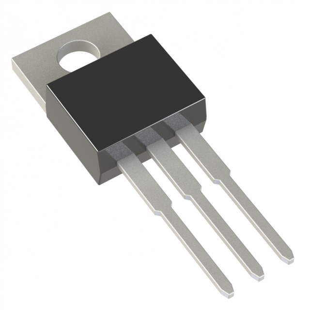
IXTP56N15T N-Channel 150V 56A MOSFET Equivalent & Substitute Parts
Part Overview
The IXTP56N15T is an N-Channel MOSFET manufactured by IXYS, designed for high-current switching applications requiring 150V drain-to-source voltage capability. This device operates in the Trench series and is rated for 56A continuous drain current at 25°C with 300W maximum power dissipation. The part maintains Active product status with full RoHS3 compliance and unlimited moisture sensitivity rating.
Substitute parts are identified when equivalent electrical performance can be achieved within the specified parameter ranges while maintaining compatible package configurations and thermal characteristics. Alternative devices may be required due to inventory availability, supply chain considerations, or application-specific thermal management needs.
Substiute Parts
Key Parameters
| Parameter | Value | Unit |
|---|---|---|
| Drain-to-Source Voltage (Vdss) | 150 | V |
| Continuous Drain Current (Id) @ 25°C | 56 | A (Tc) |
| On-State Resistance (Rds On) @ 28A, 10V | 36 | mOhm |
| Gate Threshold Voltage (Vgs(th)) @ 250µA | 4.5 | V |
| Maximum Power Dissipation (Tc) | 300 | W |
| Operating Temperature Range | -55 to 175 | °C (TJ) |
| Package Type | TO-220-3 | Through Hole |
| Gate Charge (Qg) @ 10V | 34 | nC |
| Input Capacitance (Ciss) @ 25V | 2250 | pF |
Substitute Part Grouping Explanation
Substitution eligibility for the IXTP56N15T is determined by the following critical parameters:
Mandatory Matching Criteria:
- Drain-to-Source Voltage (Vdss): 150V minimum
- Package Configuration: TO-220-3 Through Hole
- FET Type: N-Channel
- Technology: MOSFET (Metal Oxide)
- Operating Temperature Range: -55°C to 175°C minimum
Performance Compatibility Criteria:
- On-State Resistance (Rds On): Equivalent or lower at specified gate voltage
- Continuous Drain Current (Id): Equal to or exceeding application requirements
- Maximum Power Dissipation: Sufficient for thermal management in target application
- Gate Threshold Voltage (Vgs(th)): Within compatible drive voltage range
Compliance Requirements:
- RoHS3 Compliance: Required
- REACH Status: Unaffected
- Product Status: Active
The substitute parts listed below satisfy these criteria within the electrical and mechanical constraints of the IXTP56N15T application space.
Parameter Comparison
| Parameter | IXTP56N15T (Main) | FDP2552 | IRFB4615PBF | IRFB5615PBF | Unit |
|---|---|---|---|---|---|
| Manufacturer | IXYS | onsemi | Infineon Technologies | Infineon Technologies | — |
| Drain-to-Source Voltage (Vdss) | 150 | 150 | 150 | 150 | V |
| Continuous Drain Current (Id) @ 25°C | 56 (Tc) | 37 (Tc) | 35 (Tc) | 35 (Tc) | A |
| On-State Resistance (Rds On) @ 10V | 36 @ 28A | 36 @ 16A | 39 @ 21A | 39 @ 21A | mOhm |
| Gate Threshold Voltage (Vgs(th)) @ 250µA | 4.5 | 4.0 | 5.0 | 5.0 | V |
| Maximum Power Dissipation (Tc) | 300 | 150 | 144 | 144 | W |
| Gate Charge (Qg) @ 10V | 34 | 51 | 26 | 40 | nC |
| Input Capacitance (Ciss) | 2250 @ 25V | 2800 @ 25V | 1750 @ 50V | 1750 @ 50V | pF |
| Operating Temperature Range | -55 to 175 | -55 to 175 | -55 to 175 | -55 to 175 | °C (TJ) |
| Package Type | TO-220-3 | TO-220-3 | TO-220AB | TO-220AB | — |
| RoHS3 Compliance | Yes | Yes | Yes | Yes | — |
| Product Status | Active | Active | Active | Active | — |
Engineering Selection Recommendations
IXTP56N15T (Primary Reference)
The IXTP56N15T remains the primary specification reference with the highest continuous drain current rating (56A) and maximum power dissipation (300W). This device is suitable for applications requiring maximum current handling and thermal performance within the 150V class. Active product status and full RoHS3 compliance support long-term availability and regulatory requirements.
FDP2552 (onsemi PowerTrench®)
The FDP2552 provides equivalent Vdss (150V) and comparable Rds On (36 mOhm @ 16A, 10V) with reduced continuous drain current (37A Tc) and lower power dissipation (150W Tc). This substitute is applicable to applications where current requirements do not exceed 37A and thermal dissipation is limited to 150W. Active product status and RoHS3 compliance are maintained. Gate charge is elevated (51 nC @ 10V) relative to the main part.
IRFB4615PBF (Infineon HEXFET®)
The IRFB4615PBF maintains 150V Vdss with 35A continuous drain current and 144W power dissipation. On-state resistance is 39 mOhm @ 21A, 10V. This device is suitable for applications with current requirements up to 35A and thermal budgets of 144W. Gate charge is lower (26 nC @ 10V) compared to the main part, reducing switching losses. Active product status and RoHS3 compliance are confirmed.
IRFB5615PBF (Infineon)
The IRFB5615PBF provides identical electrical specifications to the IRFB4615PBF with 150V Vdss, 35A continuous drain current, and 144W power dissipation. On-state resistance is 39 mOhm @ 21A, 10V. Gate charge is 40 nC @ 10V. This device is applicable to the same current and thermal constraints as the IRFB4615PBF. Active product status and RoHS3 compliance are maintained.
All substitute parts maintain Active product status, RoHS3 compliance, REACH unaffected status, and EAR99 export classification consistent with the main part.
Frequently Asked Questions (FAQ)
Q: Can the FDP2552 be used as a direct replacement for the IXTP56N15T?
A: The FDP2552 is electrically compatible within applications requiring continuous drain current up to 37A and power dissipation up to 150W. The 150V Vdss rating and TO-220-3 package are identical. However, the reduced current and power ratings make this substitute suitable only for lower-power variants of the same application. Gate charge is higher (51 nC vs. 34 nC), which may affect switching frequency performance.
Q: What are the key differences between IRFB4615PBF and IRFB5615PBF?
A: Both devices share identical electrical specifications: 150V Vdss, 35A continuous drain current, 39 mOhm Rds On @ 21A, 10V, and 144W power dissipation. The primary difference is gate charge: IRFB4615PBF is rated at 26 nC @ 10V, while IRFB5615PBF is rated at 40 nC @ 10V. Both are packaged in TO-220AB and maintain Active product status with RoHS3 compliance.
Q: Are all substitute parts available in the same package configuration?
A: The FDP2552 is packaged in TO-220-3, matching the main part exactly. The IRFB4615PBF and IRFB5615PBF are packaged in TO-220AB, which is mechanically compatible with TO-220-3 applications using standard through-hole mounting. Pin configurations remain consistent across all devices.
Q: What is the impact of different gate charge ratings on circuit design?
A: Gate charge (Qg) affects switching speed and driver circuit requirements. The IXTP56N15T has 34 nC @ 10V, FDP2552 has 51 nC @ 10V, IRFB4615PBF has 26 nC @ 10V, and IRFB5615PBF has 40 nC @ 10V. Higher gate charge requires longer switching times or higher gate drive current. Lower gate charge reduces switching losses and allows faster switching frequencies. Circuit design must account for these differences in gate driver capability.
Q: Are all substitute parts RoHS3 compliant?
A: Yes. The IXTP56N15T, FDP2552, IRFB4615PBF, and IRFB5615PBF are all RoHS3 compliant. All devices maintain REACH unaffected status and EAR99 export classification.
Q: What thermal considerations apply when selecting a substitute?
A: Maximum power dissipation ratings differ significantly: IXTP56N15T (300W), FDP2552 (150W), IRFB4615PBF (144W), and IRFB5615PBF (144W). Applications with thermal dissipation exceeding 150W require the main part or equivalent high-power devices. All devices operate across -55°C to 175°C junction temperature range, supporting identical thermal operating windows.
Q: Can substitute parts be used in high-frequency switching applications?
A: Gate charge and input capacitance affect high-frequency performance. The IRFB4615PBF offers the lowest gate charge (26 nC @ 10V) and lowest input capacitance (1750 pF @ 50V), making it optimal for high-frequency applications. The FDP2552 has higher gate charge (51 nC @ 10V) and higher input capacitance (2800 pF @ 25V), which may limit switching frequency. Circuit design must verify gate driver capability and switching losses at target frequencies.
Alternative Parts

SJ6012L2TP
Littelfuse Inc.
6 Alternative Parts

JMK107BBJ476MA-RE
Taiyo Yuden
10 Alternative Parts

GMK107BBJ475MA-T
Taiyo Yuden
5 Alternative Parts
SJ6020N2ARP
Littelfuse Inc.
3 Alternative Parts
SJ6025R2ATP
Littelfuse Inc.
4 Alternative Parts

2474-05L
API Delevan Inc.
1 Alternative Parts

4590R-684K
API Delevan Inc.
1 Alternative Parts

CM6560R-334
API Delevan Inc.
1 Alternative Parts

CM6460-104
API Delevan Inc.
1 Alternative Parts

5526-12
API Delevan Inc.
1 Alternative Parts