


Request Quote
(Ships tomorrow)
IXTP1R6N50P N-Channel MOSFET Equivalent & Substitute Parts
Part Overview
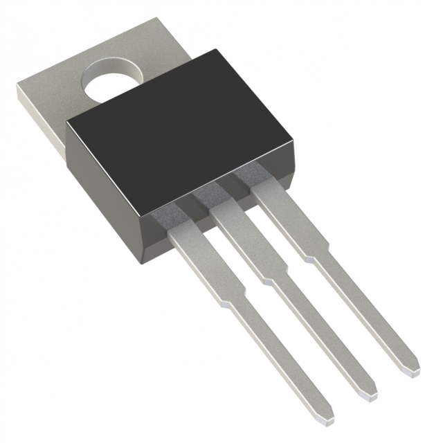
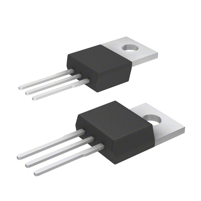
The IXTP1R6N50P is an N-Channel MOSFET manufactured by IXYS, rated for 500V drain-to-source voltage with 1.6A continuous drain current at 25°C. This device is packaged in a Through Hole TO-220-3 configuration and is designed for high-voltage switching applications. The part is classified as Obsolete, making identification of functionally equivalent alternatives necessary for ongoing design support and procurement.
Substiute Parts
Key Parameters
| Parameter | Value | Unit |
|---|---|---|
| Drain to Source Voltage (Vdss) | 500 | V |
| Continuous Drain Current (Id) @ 25°C | 1.6 | A |
| Rds On (Max) @ 500mA, 10V | 6.5 | Ohm |
| Gate Threshold Voltage (Vgs(th)) @ 25µA | 5.5 | V |
| Power Dissipation (Max) | 43 | W |
| Operating Temperature Range | -55 to 150 | °C |
| Package Type | TO-220-3 | — |
| Mounting Type | Through Hole | — |
Substitute Part Grouping Explanation
Substitution of the IXTP1R6N50P is determined by the following electrical and mechanical parameters:
Mandatory Compatibility Criteria:
- FET Type: N-Channel
- Technology: MOSFET (Metal Oxide)
- Mounting Type: Through Hole
- Package Type: TO-220 family
- Gate Drive Voltage: 10V
- Maximum Gate Voltage: ±30V
- Operating Temperature Range: -55°C to 150°C
Functional Substitution Parameters:
- Drain-to-Source Voltage (Vdss) must equal or exceed 500V
- Continuous Drain Current (Id) must equal or exceed 1.6A
- On-State Resistance (Rds On) should not significantly degrade circuit performance
- Power Dissipation capability must support application requirements
The IXTP2N65X2 qualifies as a substitute based on these criteria. It maintains N-Channel MOSFET topology, Through Hole mounting, TO-220 package configuration, and identical gate drive specifications. The substitute provides enhanced electrical performance with higher voltage rating (650V), increased current capability (2A), and improved thermal characteristics (55W vs. 43W).
Parameter Comparison
| Parameter | IXTP1R6N50P | IXTP2N65X2 | Unit |
|---|---|---|---|
| Manufacturer | IXYS | IXYS | — |
| FET Type | N-Channel | N-Channel | — |
| Technology | MOSFET (Metal Oxide) | MOSFET (Metal Oxide) | — |
| Drain to Source Voltage (Vdss) | 500 | 650 | V |
| Continuous Drain Current (Id) @ 25°C | 1.6 | 2.0 | A |
| Drive Voltage (Max Rds On) | 10 | 10 | V |
| Rds On (Max) | 6.5 @ 500mA | 2.3 @ 1A | Ohm |
| Gate Threshold Voltage (Vgs(th)) (Max) | 5.5 @ 25µA | 5.0 @ 250µA | V |
| Gate Charge (Qg) (Max) @ 10V | 3.9 | 4.3 | nC |
| Maximum Gate Voltage (Vgs) | ±30 | ±30 | V |
| Input Capacitance (Ciss) (Max) @ 25V | 140 | 180 | pF |
| Power Dissipation (Max) | 43 | 55 | W |
| Operating Temperature Range | -55 to 150 | -55 to 150 | °C |
| Mounting Type | Through Hole | Through Hole | — |
| Package Type | TO-220-3 | TO-220-3 | — |
| RoHS Status | ROHS3 Compliant | ROHS3 Compliant | — |
| REACH Status | REACH Unaffected | REACH Unaffected | — |
| Product Status | Obsolete | Active | — |
Engineering Selection Recommendations
IXTP1R6N50P (Original Part): The IXTP1R6N50P is classified as Obsolete. While ROHS3 Compliant and REACH Unaffected, the obsolete status limits long-term availability and future procurement viability. Current inventory of 763 pieces is available; however, this represents a finite supply.
IXTP2N65X2 (Substitute Part): The IXTP2N65X2 is classified as Active and maintains full regulatory compliance (ROHS3 Compliant, REACH Unaffected). This part is manufactured by the same supplier (IXYS) and provides superior electrical performance across all critical parameters. The Active product status ensures ongoing availability and manufacturing support. The substitute is suitable for direct replacement in applications where the original IXTP1R6N50P was specified, provided circuit design accommodates the enhanced voltage and current ratings.
Frequently Asked Questions (FAQ)
Q: Can the IXTP2N65X2 directly replace the IXTP1R6N50P in existing designs?
A: Yes. Both devices share identical gate drive voltage (10V), maximum gate voltage (±30V), operating temperature range (-55°C to 150°C), and Through Hole TO-220-3 package configuration. The IXTP2N65X2 provides higher voltage (650V vs. 500V) and current (2A vs. 1.6A) ratings, making it functionally compatible for applications designed around the IXTP1R6N50P specifications.
Q: What are the key differences between these two MOSFETs?
A: The IXTP2N65X2 provides enhanced performance: 650V drain-to-source voltage (vs. 500V), 2A continuous drain current (vs. 1.6A), lower on-state resistance (2.3 Ohm vs. 6.5 Ohm), and higher power dissipation capability (55W vs. 43W). The IXTP1R6N50P is Obsolete; the IXTP2N65X2 is Active.
Q: Are there package compatibility concerns?
A: Both devices use Through Hole TO-220-3 packaging. Pin configuration and mechanical dimensions are compatible, allowing direct PCB mounting without layout modifications.
Q: What is the impact of the lower on-state resistance in the substitute?
A: The IXTP2N65X2 exhibits lower on-state resistance (2.3 Ohm @ 1A vs. 6.5 Ohm @ 500mA), resulting in reduced conduction losses and improved thermal efficiency. This characteristic benefits high-frequency switching applications and reduces heat dissipation requirements.
Q: Does the higher gate charge affect circuit operation?
A: Gate charge increases from 3.9 nC to 4.3 nC. This minimal difference (approximately 10%) has negligible impact on gate drive circuit design and switching speed for typical applications.
Q: Are regulatory certifications equivalent?
A: Yes. Both parts are ROHS3 Compliant and REACH Unaffected, meeting identical environmental and regulatory requirements.
Alternative Parts

SJ6012L2TP
Littelfuse Inc.
6 Alternative Parts

JMK107BBJ476MA-RE
Taiyo Yuden
10 Alternative Parts

GMK107BBJ475MA-T
Taiyo Yuden
5 Alternative Parts
SJ6020N2ARP
Littelfuse Inc.
3 Alternative Parts
SJ6025R2ATP
Littelfuse Inc.
4 Alternative Parts

2474-05L
API Delevan Inc.
1 Alternative Parts

4590R-684K
API Delevan Inc.
1 Alternative Parts

CM6560R-334
API Delevan Inc.
1 Alternative Parts

CM6460-104
API Delevan Inc.
1 Alternative Parts

5526-12
API Delevan Inc.
1 Alternative Parts