


Request Quote
(Ships tomorrow)
IXTP1R6N50D2 Equivalent & Substitute Parts
Part Overview
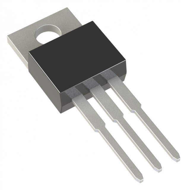
The IXTP1R6N50D2 is an N-Channel depletion-mode MOSFET manufactured by IXYS, rated for 500V drain-to-source voltage with 1.6A continuous drain current at 25°C. This device is packaged in a TO-220-3 through-hole configuration and is designed for high-voltage switching applications requiring 100W power dissipation capability. The part maintains Active product status with full RoHS3 compliance and unlimited moisture sensitivity rating.
Substitute parts are identified when equivalent electrical performance can be achieved within the specified voltage, current, and thermal operating ranges while maintaining compatible package footprints or acceptable mechanical alternatives.
Substiute Parts
Key Parameters
| Parameter | Value | Unit |
|---|---|---|
| Drain to Source Voltage (Vdss) | 500 | V |
| Continuous Drain Current (Id) @ 25°C | 1.6 | A |
| Power Dissipation (Max) | 100 | W |
| Rds On (Max) @ 800mA, 0V | 2.3 | Ohm |
| Gate Charge (Qg) @ 5V | 23.7 | nC |
| Input Capacitance (Ciss) @ 25V | 645 | pF |
| Operating Temperature Range | -55 to 150 | °C |
| Package Type | TO-220-3 | Through Hole |
| FET Type | N-Channel | |
| FET Feature | Depletion Mode |
Substitute Part Grouping Explanation
Substitution eligibility for the IXTP1R6N50D2 is determined by the following critical parameters:
Voltage Rating: The substitute must maintain a Drain-to-Source Voltage (Vdss) rating equal to or greater than 500V to ensure safe operation in the intended application voltage domain.
Current Capacity: The substitute must support a continuous drain current (Id) at 25°C equal to or greater than 1.6A to handle the specified load without thermal stress.
Power Dissipation: The substitute must be capable of dissipating at least 100W at the case temperature (Tc) to maintain thermal stability under full-load conditions.
On-State Resistance (Rds On): The substitute's maximum on-state resistance must not significantly exceed 2.3 Ohm to prevent excessive conduction losses and heat generation.
Gate Charge (Qg): Lower gate charge values reduce switching losses and improve circuit efficiency; however, substitutes with higher gate charge remain functionally compatible.
Input Capacitance (Ciss): This parameter affects switching speed and gate drive requirements; substitutes with different capacitance values remain compatible if gate drive circuitry is appropriately designed.
Package Compatibility: The primary package is TO-220-3 through-hole. Substitutes in alternative through-hole packages (such as I-PAK/TO-251) are acceptable if mechanical mounting and thermal management requirements are satisfied.
Temperature Range: The substitute must support the full operating temperature range of -55°C to 150°C (TJ).
Parameter Comparison
| Parameter | IXTP1R6N50D2 (Main) | STU4N52K3 (Substitute) | Unit |
|---|---|---|---|
| Manufacturer | IXYS | STMicroelectronics | |
| Drain to Source Voltage (Vdss) | 500 | 525 | V |
| Continuous Drain Current (Id) @ 25°C | 1.6 | 2.5 | A |
| Power Dissipation (Max) | 100 | 45 | W |
| Rds On (Max) | 2.3 @ 800mA, 0V | 2.6 @ 1.25A, 10V | Ohm |
| Gate Charge (Qg) (Max) | 23.7 @ 5V | 11 @ 10V | nC |
| Input Capacitance (Ciss) (Max) | 645 @ 25V | 334 @ 100V | pF |
| Vgs (Max) | ±20 | ±30 | V |
| Operating Temperature Range | -55 to 150 | -55 to 150 | °C |
| Package Type | TO-220-3 | I-PAK (TO-251-3) | |
| FET Type | N-Channel | N-Channel | |
| Product Status | Active | Active | |
| RoHS Status | ROHS3 Compliant | ROHS3 Compliant | |
| REACH Status | REACH Unaffected | REACH Unaffected |
Engineering Selection Recommendations
STU4N52K3 as a Substitute for IXTP1R6N50D2
The STU4N52K3 from STMicroelectronics meets the primary electrical requirements for substitution:
The STU4N52K3 provides a Vdss rating of 525V, which exceeds the 500V requirement of the IXTP1R6N50D2, ensuring adequate voltage margin. The continuous drain current rating of 2.5A at 25°C exceeds the 1.6A specification, providing additional current capacity.
Both devices maintain Active product status and full RoHS3 compliance with REACH Unaffected designation, ensuring regulatory alignment for new designs and existing applications.
The STU4N52K3 exhibits lower gate charge (11 nC versus 23.7 nC) and reduced input capacitance (334 pF versus 645 pF), resulting in improved switching efficiency and reduced gate drive power requirements.
The primary consideration is the reduced power dissipation rating of the STU4N52K3 (45W versus 100W). Applications requiring sustained power dissipation above 45W at the case temperature must employ enhanced thermal management or confirm that actual operating conditions remain within the substitute's thermal envelope.
The STU4N52K3 is packaged in I-PAK (TO-251-3) format rather than TO-220-3. This package change requires mechanical redesign of the printed circuit board layout and may affect thermal coupling to heatsinks. Pin configuration compatibility must be verified against the specific application circuit.
Frequently Asked Questions (FAQ)
Q: Can the STU4N52K3 directly replace the IXTP1R6N50D2 without circuit modifications?
A: Electrical substitution is feasible based on voltage and current ratings. However, the package change from TO-220-3 to I-PAK (TO-251-3) requires PCB layout modification. Pin-to-pin compatibility must be confirmed for the specific application. The reduced power dissipation rating (45W versus 100W) requires thermal analysis to ensure the substitute operates within its thermal limits under actual load conditions.
Q: What is the significance of the lower gate charge in the STU4N52K3?
A: Lower gate charge (11 nC versus 23.7 nC) reduces the energy required to switch the transistor on and off. This results in lower gate drive power consumption and potentially faster switching transitions, which can improve overall circuit efficiency and reduce electromagnetic interference.
Q: Are both devices suitable for high-temperature applications?
A: Both the IXTP1R6N50D2 and STU4N52K3 support the full operating temperature range of -55°C to 150°C (TJ). Selection between them for high-temperature applications depends on thermal management capability and power dissipation requirements at elevated temperatures.
Q: What does the depletion-mode feature of the IXTP1R6N50D2 indicate?
A: Depletion-mode operation means the transistor conducts in its default state (with zero gate-source voltage) and turns off when a negative gate voltage is applied. This differs from enhancement-mode devices, which require positive gate voltage to conduct. The STU4N52K3 does not specify a depletion-mode feature, indicating it operates in enhancement mode. This functional difference may affect circuit design and gate drive requirements.
Q: How do the different Rds On measurement conditions affect substitution?
A: The IXTP1R6N50D2 specifies Rds On at 800mA and 0V gate-source voltage, while the STU4N52K3 specifies it at 1.25A and 10V. These different measurement conditions reflect the devices' operational characteristics. Direct numerical comparison is not valid; however, both values indicate acceptable on-state resistance for typical switching applications. Actual performance depends on the specific gate drive voltage and current levels in the application circuit.
Q: What inventory considerations apply to these parts?
A: The IXTP1R6N50D2 has 15,226 pieces in stock, while the STU4N52K3 has 3,300 pieces available. Substitution decisions may be influenced by supply availability and lead time requirements for production schedules.
Alternative Parts

SJ6012L2TP
Littelfuse Inc.
6 Alternative Parts

JMK107BBJ476MA-RE
Taiyo Yuden
10 Alternative Parts

GMK107BBJ475MA-T
Taiyo Yuden
5 Alternative Parts
SJ6020N2ARP
Littelfuse Inc.
3 Alternative Parts
SJ6025R2ATP
Littelfuse Inc.
4 Alternative Parts

2474-05L
API Delevan Inc.
1 Alternative Parts

4590R-684K
API Delevan Inc.
1 Alternative Parts

CM6560R-334
API Delevan Inc.
1 Alternative Parts

CM6460-104
API Delevan Inc.
1 Alternative Parts

5526-12
API Delevan Inc.
1 Alternative Parts