


Request Quote
(Ships tomorrow)
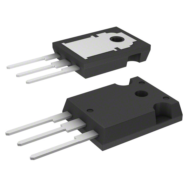
IXTH6N90A N-Channel 900V 6A MOSFET TO-247 Equivalent & Substitute Parts
Part Overview
The IXTH6N90A is an N-Channel metal oxide semiconductor field-effect transistor (MOSFET) rated for 900V drain-to-source voltage with 6A continuous drain current in a through-hole TO-247 package. Manufactured by IXYS, this device is classified as obsolete product status. Due to its obsolete classification, equivalent and substitute parts from active manufacturers are necessary to maintain design continuity and ensure long-term component availability for new production and field replacements.
Substiute Parts
Key Parameters
| Parameter | Value | Unit |
|---|---|---|
| Drain-to-Source Voltage (Vdss) | 900 | V |
| Continuous Drain Current (Id) @ 25°C | 6 | A |
| On-State Resistance (Rds On Max) @ Id, Vgs | 1.4 | Ohm @ 3A, 10V |
| Gate Threshold Voltage (Vgs(th) Max) @ Id | 4.5 | V @ 250µA |
| Gate Charge (Qg Max) @ Vgs | 130 | nC @ 10V |
| Maximum Gate Voltage (Vgs Max) | ±20 | V |
| Input Capacitance (Ciss Max) @ Vds | 2600 | pF @ 25V |
| Power Dissipation (Max) | 180 | W |
| Operating Temperature Range | -55 to 150 | °C |
| Mounting Type | Through Hole | |
| Package | TO-247-3 | |
| RoHS Status | ROHS3 Compliant |
Substitute Part Grouping Explanation
Substitution of the IXTH6N90A is determined by the following critical electrical and mechanical parameters:
Primary Substitution Criteria:
- Drain-to-Source Voltage (Vdss): Minimum 900V required
- Continuous Drain Current (Id): Minimum 6A required
- Package Type: TO-247 through-hole configuration
- FET Type: N-Channel metal oxide technology
- Operating Temperature Range: -55°C to 150°C minimum
- RoHS3 Compliance: Required for regulatory alignment
Secondary Compatibility Parameters:
- On-State Resistance (Rds On): Lower or equivalent values acceptable
- Gate Threshold Voltage (Vgs(th)): Within ±0.5V tolerance acceptable
- Gate Charge (Qg): Lower values acceptable for improved switching performance
- Maximum Gate Voltage (Vgs Max): ±20V minimum required
Substitute parts are grouped into two categories:
Category A - Direct Voltage Class Substitutes (900V Rating): STW7NK90Z, STW9NK90Z, STW11NK90Z, STW12NK90Z (STMicroelectronics SuperMESH™ series). These devices maintain the 900V Vdss rating with enhanced current ratings and improved on-state resistance characteristics.
Category B - Higher Voltage Class Substitutes (1000V Rating): APT8M100B (Microchip Technology), FQH8N100C (onsemi QFET®). These devices provide higher voltage margin with 1000V Vdss rating, suitable for applications requiring additional voltage headroom.
Parameter Comparison
| Parameter | IXTH6N90A | STW7NK90Z | STW9NK90Z | STW11NK90Z | STW12NK90Z | APT8M100B | FQH8N100C |
|---|---|---|---|---|---|---|---|
| Manufacturer | IXYS | STMicroelectronics | STMicroelectronics | STMicroelectronics | STMicroelectronics | Microchip Technology | onsemi |
| Vdss (V) | 900 | 900 | 900 | 900 | 900 | 1000 | 1000 |
| Id @ 25°C (A) | 6 | 5.8 | 8 | 9.2 | 11 | 8 | 8 |
| Rds On Max (Ohm) | 1.4 @ 3A, 10V | 2 @ 2.9A, 10V | 1.3 @ 3.6A, 10V | 0.98 @ 4.6A, 10V | 0.88 @ 5.5A, 10V | 1.8 @ 4A, 10V | 1.45 @ 4A, 10V |
| Vgs(th) Max (V) | 4.5 @ 250µA | 4.5 @ 100µA | 4.5 @ 100µA | 4.5 @ 100µA | 4.5 @ 100µA | 5 @ 1mA | 5 @ 250µA |
| Qg Max (nC) | 130 @ 10V | 60.5 @ 10V | 72 @ 10V | 115 @ 10V | 152 @ 10V | 60 @ 10V | 70 @ 10V |
| Vgs Max (V) | ±20 | ±30 | ±30 | ±30 | ±30 | ±30 | ±30 |
| Ciss Max (pF) | 2600 @ 25V | 1350 @ 25V | 2115 @ 25V | 3000 @ 25V | 3500 @ 25V | 1885 @ 25V | 3220 @ 25V |
| Power Dissipation Max (W) | 180 | 140 | 160 | 200 | 230 | 290 | 225 |
| Operating Temperature (°C) | -55 to 150 | -55 to 150 | -55 to 150 | -55 to 150 | -55 to 150 | -55 to 150 | -55 to 150 |
| Package | TO-247-3 | TO-247-3 | TO-247-3 | TO-247-3 | TO-247-3 | TO-247 [B] | TO-247-3 |
| Product Status | Obsolete | Active | Active | Active | Active | Active | Active |
| RoHS Status | ROHS3 Compliant | ROHS3 Compliant | ROHS3 Compliant | ROHS3 Compliant | ROHS3 Compliant | ROHS3 Compliant | ROHS3 Compliant |
Engineering Selection Recommendations
For Direct Replacement (900V Voltage Class):
STW9NK90Z is the primary substitute for the IXTH6N90A. This STMicroelectronics SuperMESH™ device maintains the 900V Vdss rating with 8A continuous drain current, exceeding the original 6A specification. The on-state resistance of 1.3 Ohm at 3.6A, 10V is superior to the IXTH6N90A specification. Product status is active with ROHS3 compliance and unlimited moisture sensitivity level. Gate charge of 72 nC provides improved switching characteristics compared to the original 130 nC specification.
STW7NK90Z provides a conservative substitute with 5.8A continuous drain current, slightly below the original 6A rating. This device is suitable for applications where current margin is not critical. On-state resistance of 2 Ohm is higher than the original specification but acceptable for lower-power applications.
STW11NK90Z and STW12NK90Z offer enhanced performance with 9.2A and 11A continuous drain current ratings respectively, with superior on-state resistance characteristics (0.98 Ohm and 0.88 Ohm). These devices are suitable for applications requiring higher current capacity or improved thermal performance.
For Higher Voltage Margin Applications (1000V Voltage Class):
APT8M100B (Microchip Technology) provides 1000V Vdss with 8A continuous drain current and 290W power dissipation. This device is suitable for applications requiring additional voltage headroom. On-state resistance of 1.8 Ohm is acceptable for most applications. Product status is active with ROHS3 compliance.
FQH8N100C (onsemi QFET®) provides 1000V Vdss with 8A continuous drain current and 225W power dissipation. On-state resistance of 1.45 Ohm is superior to APT8M100B. Product status is active with ROHS3 compliance. This device is suitable for applications requiring higher voltage rating with improved on-state resistance performance.
Selection Criteria Summary:
All substitute parts meet the mandatory requirements of N-Channel metal oxide technology, through-hole TO-247 package configuration, -55°C to 150°C operating temperature range, and ROHS3 compliance. All substitute parts are classified as active product status, ensuring long-term availability and manufacturing support. Selection between substitute parts depends on specific application requirements for current rating, on-state resistance, power dissipation, and voltage margin.
Frequently Asked Questions (FAQ)
Q: Can STW7NK90Z be used as a direct replacement for IXTH6N90A?
A: STW7NK90Z is electrically compatible with the IXTH6N90A for applications where the 5.8A continuous drain current rating is sufficient. The device maintains the 900V Vdss rating and TO-247-3 package configuration. However, the on-state resistance of 2 Ohm is higher than the original 1.4 Ohm specification, resulting in increased power dissipation. Thermal analysis is required to confirm suitability for the specific application.
Q: What is the advantage of using STW9NK90Z over STW7NK90Z?
A: STW9NK90Z provides 8A continuous drain current compared to STW7NK90Z at 5.8A, offering 38% higher current capacity. The on-state resistance of 1.3 Ohm is significantly lower than STW7NK90Z at 2 Ohm, resulting in reduced power dissipation and improved thermal performance. Gate charge of 72 nC is lower than the original IXTH6N90A at 130 nC, enabling faster switching operation.
Q: Are APT8M100B and FQH8N100C suitable for applications designed for 900V operation?
A: APT8M100B and FQH8N100C are rated for 1000V Vdss, providing 100V additional voltage margin above the original 900V specification. These devices are suitable for applications designed for 900V operation and provide enhanced voltage headroom for transient overvoltage conditions. The higher voltage rating does not negatively impact performance in 900V applications.
Q: What is the difference between TO-247 [B] and TO-247-3 packages?
A: Both TO-247 [B] and TO-247-3 are through-hole packages with identical pin configuration and mechanical dimensions. The designations refer to different manufacturer package specifications. APT8M100B uses TO-247 [B] designation while other substitute parts use TO-247-3 designation. Both packages are mechanically and electrically interchangeable for PCB mounting and circuit operation.
Q: Why is the gate charge specification important for substitution?
A: Gate charge (Qg) determines the amount of charge required to switch the MOSFET from off-state to on-state. Lower gate charge enables faster switching operation and reduces gate drive circuit power consumption. The IXTH6N90A specifies 130 nC gate charge, while substitute parts range from 60 nC to 152 nC. Devices with lower gate charge (STW7NK90Z at 60.5 nC, APT8M100B at 60 nC) provide improved switching performance.
Q: Can STW12NK90Z be used in applications where thermal dissipation is critical?
A: STW12NK90Z provides the highest power dissipation rating at 230W among the 900V substitute options, with the lowest on-state resistance of 0.88 Ohm at 5.5A, 10V. This combination results in reduced power dissipation per ampere of drain current, making it suitable for high-current applications where thermal management is critical. The device is recommended for applications requiring maximum thermal performance within the 900V voltage class.
Q: What compliance certifications are maintained across all substitute parts?
A: All substitute parts maintain ROHS3 compliance and REACH unaffected status, identical to the original IXTH6N90A. All devices are classified under ECCN EAR99 and HTSUS 8541.29.0095 for export and tariff purposes. Moisture sensitivity level is 1 (unlimited) for all STMicroelectronics devices, indicating no moisture sensitivity restrictions during storage and handling.
Q: Is the higher Vgs Max rating of substitute parts (±30V vs ±20V) a concern?
A: The higher Vgs Max rating of ±30V on substitute parts provides additional gate voltage margin compared to the original IXTH6N90A at ±20V. This is not a concern and does not negatively impact compatibility. Gate drive circuits designed for ±20V operation function correctly with devices rated for ±30V. The higher rating provides additional safety margin for gate drive circuit design.
Alternative Parts

SJ6012L2TP
Littelfuse Inc.
6 Alternative Parts

JMK107BBJ476MA-RE
Taiyo Yuden
10 Alternative Parts

GMK107BBJ475MA-T
Taiyo Yuden
5 Alternative Parts
SJ6020N2ARP
Littelfuse Inc.
3 Alternative Parts
SJ6025R2ATP
Littelfuse Inc.
4 Alternative Parts

2474-05L
API Delevan Inc.
1 Alternative Parts

4590R-684K
API Delevan Inc.
1 Alternative Parts

CM6560R-334
API Delevan Inc.
1 Alternative Parts

CM6460-104
API Delevan Inc.
1 Alternative Parts

5526-12
API Delevan Inc.
1 Alternative Parts