


Request Quote
(Ships tomorrow)
IXFR10N100Q Equivalent & Substitute Parts
Part Overview
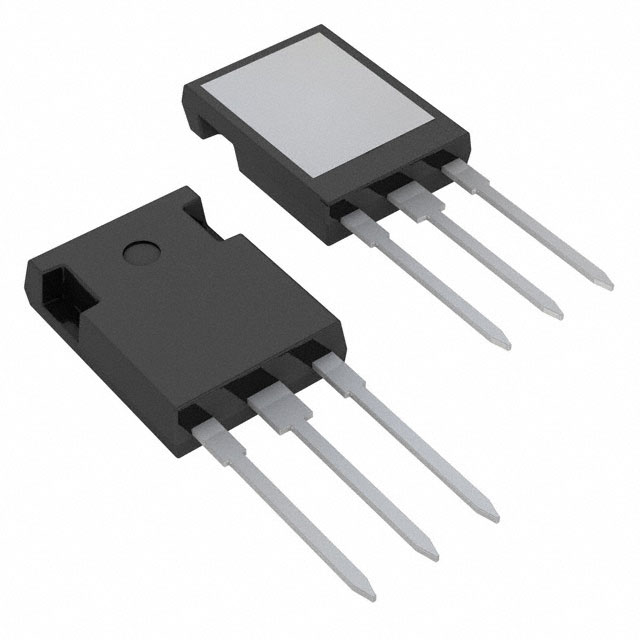
The IXFR10N100Q is an N-Channel MOSFET manufactured by IXYS, rated for 1000V drain-to-source voltage with 9A continuous drain current at 25°C. This device is part of the HiPerFET™ Q Class series and is housed in an ISOPLUS247™ package (TO-247-3 form factor). The component is designed for high-voltage switching applications requiring robust thermal performance with a maximum power dissipation of 250W at the case temperature.
The IXFR10N100Q maintains Active product status with full RoHS3 compliance and unlimited moisture sensitivity rating. Substitute components are identified based on matching critical electrical parameters including drain-to-source voltage rating, continuous drain current, gate-source voltage specifications, and compatible through-hole packaging.
Substiute Parts
Key Parameters
| Parameter | Value | Unit |
|---|---|---|
| Drain to Source Voltage (Vdss) | 1000 | V |
| Current - Continuous Drain (Id) @ 25°C | 9 | A |
| Drive Voltage (Max Rds On) | 10 | V |
| Rds On (Max) @ Id, Vgs | 1.2 | Ohm @ 5A, 10V |
| Vgs(th) (Max) @ Id | 5.5 | V @ 4mA |
| Gate Charge (Qg) (Max) @ Vgs | 90 | nC @ 10V |
| Vgs (Max) | ±20 | V |
| Input Capacitance (Ciss) (Max) @ Vds | 2900 | pF @ 25V |
| Power Dissipation (Max) | 250 | W |
| Operating Temperature | -55 to 150 | °C |
| Mounting Type | Through Hole | - |
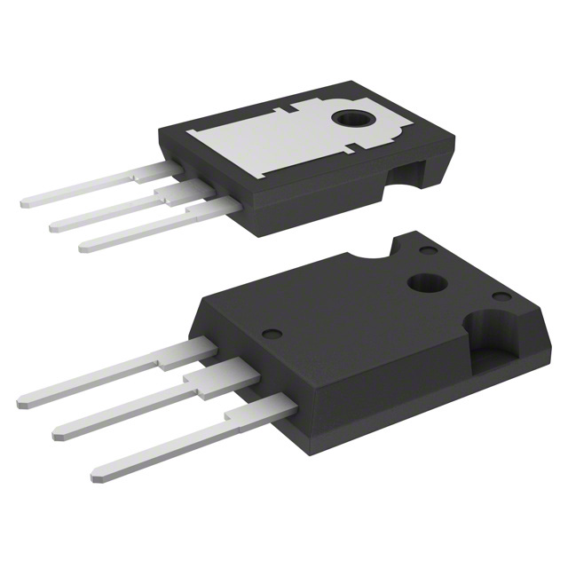
| Package / Case | TO-247-3 | - |
| FET Type | N-Channel | - |
| Technology | MOSFET (Metal Oxide) | - |
Substitute Part Grouping Explanation
Substitute components for the IXFR10N100Q are identified based on strict electrical and mechanical compatibility criteria. The primary substitution logic is based on the following parameters:
Critical Matching Parameters:
- FET Type: N-Channel configuration
- Technology: MOSFET (Metal Oxide)
- Mounting Type: Through Hole
- Package / Case: TO-247-3 form factor
- Drain to Source Voltage (Vdss): Rated for high-voltage operation (950V minimum)
- Current - Continuous Drain (Id) @ 25°C: 9A minimum
- Drive Voltage: 10V gate drive compatibility
- Operating Temperature Range: -55°C to 150°C
- Compliance: RoHS3 compliant, REACH unaffected
The STW6N95K5 from STMicroelectronics meets these criteria with a 950V Vdss rating, 9A continuous drain current, TO-247-3 package, and identical operating temperature range. Both devices are Active products with full regulatory compliance.
Parameter Comparison
| Parameter | IXFR10N100Q (Main) | STW6N95K5 (Substitute) | Unit |
|---|---|---|---|
| Manufacturer | IXYS | STMicroelectronics | - |
| FET Type | N-Channel | N-Channel | - |
| Technology | MOSFET (Metal Oxide) | MOSFET (Metal Oxide) | - |
| Drain to Source Voltage (Vdss) | 1000 | 950 | V |
| Current - Continuous Drain (Id) @ 25°C | 9 | 9 | A |
| Drive Voltage (Max Rds On) | 10 | 10 | V |
| Rds On (Max) @ Id, Vgs | 1.2 @ 5A, 10V | 1.25 @ 3A, 10V | Ohm |
| Vgs(th) (Max) @ Id | 5.5 @ 4mA | 5 @ 100µA | V |
| Gate Charge (Qg) (Max) @ Vgs | 90 @ 10V | 13 @ 10V | nC |
| Vgs (Max) | ±20 | ±30 | V |
| Input Capacitance (Ciss) (Max) @ Vds | 2900 @ 25V | 450 @ 100V | pF |
| Power Dissipation (Max) | 250 | 90 | W |
| Operating Temperature | -55 to 150 | -55 to 150 | °C |
| Mounting Type | Through Hole | Through Hole | - |
| Package / Case | TO-247-3 | TO-247-3 | - |
| Product Status | Active | Active | - |
| RoHS Status | ROHS3 Compliant | ROHS3 Compliant | - |
| REACH Status | REACH Unaffected | REACH Unaffected | - |
Engineering Selection Recommendations
Primary Component (IXFR10N100Q): The IXFR10N100Q is the specified component with 1000V Vdss rating, 250W power dissipation capability, and HiPerFET™ Q Class technology. This device is suitable for applications requiring maximum voltage headroom and thermal performance. Active product status ensures continued availability and support.
Substitute Component (STW6N95K5): The STW6N95K5 is a functionally equivalent substitute for applications where the 950V Vdss rating is sufficient. This device features SuperMESH5™ technology with lower gate charge (13 nC versus 90 nC), reduced input capacitance (450 pF versus 2900 pF), and higher maximum gate-source voltage (±30V versus ±20V). The STW6N95K5 is rated for 90W maximum power dissipation, which is lower than the IXFR10N100Q.
Selection Criteria: Both components are Active products with RoHS3 compliance and REACH unaffected status. Selection between these devices depends on application voltage requirements and thermal design constraints. The IXFR10N100Q provides higher voltage margin and thermal capacity. The STW6N95K5 offers improved switching characteristics with lower gate charge and input capacitance, beneficial for high-frequency switching applications.
Frequently Asked Questions (FAQ)
Q: Can the STW6N95K5 be used as a direct replacement for the IXFR10N100Q?
A: The STW6N95K5 is electrically compatible for applications operating at or below 950V. Both devices share identical continuous drain current (9A), operating temperature range (-55°C to 150°C), and TO-247-3 package. However, the STW6N95K5 has a lower maximum power dissipation rating (90W versus 250W), which may limit its use in high-power thermal environments.
Q: What is the voltage difference between these two MOSFETs?
A: The IXFR10N100Q is rated for 1000V drain-to-source voltage, while the STW6N95K5 is rated for 950V. This 50V difference represents a 5% reduction in voltage rating. Applications operating below 950V can use either device; applications requiring the full 1000V rating must use the IXFR10N100Q.
Q: Are both devices available in the same package?
A: Yes. Both the IXFR10N100Q and STW6N95K5 use the TO-247-3 package with through-hole mounting. Pin configuration and mechanical dimensions are compatible for direct board-level substitution.
Q: What are the key differences in gate charge specifications?
A: The IXFR10N100Q has a maximum gate charge of 90 nC at 10V, while the STW6N95K5 has 13 nC at 10V. The lower gate charge of the STW6N95K5 results in faster switching transitions and reduced gate drive power requirements, making it advantageous for high-frequency applications.
Q: How do the input capacitance values compare?
A: The IXFR10N100Q has 2900 pF input capacitance at 25V, while the STW6N95K5 has 450 pF at 100V. The significantly lower input capacitance of the STW6N95K5 reduces capacitive loading on the gate drive circuit and improves switching speed.
Q: Are both devices RoHS3 compliant?
A: Yes. Both the IXFR10N100Q and STW6N95K5 are RoHS3 compliant and REACH unaffected, meeting current environmental and regulatory requirements.
Q: What is the maximum gate-source voltage for each device?
A: The IXFR10N100Q is rated for ±20V maximum gate-source voltage, while the STW6N95K5 is rated for ±30V. The higher rating of the STW6N95K5 provides additional margin for gate drive circuit design.
Q: Which device should be selected for thermal-constrained applications?
A: The IXFR10N100Q is rated for 250W maximum power dissipation, compared to 90W for the STW6N95K5. Applications with significant thermal requirements should use the IXFR10N100Q to ensure adequate heat dissipation capability.
Alternative Parts

SJ6012L2TP
Littelfuse Inc.
6 Alternative Parts

JMK107BBJ476MA-RE
Taiyo Yuden
10 Alternative Parts

GMK107BBJ475MA-T
Taiyo Yuden
5 Alternative Parts
SJ6020N2ARP
Littelfuse Inc.
3 Alternative Parts
SJ6025R2ATP
Littelfuse Inc.
4 Alternative Parts

2474-05L
API Delevan Inc.
1 Alternative Parts

4590R-684K
API Delevan Inc.
1 Alternative Parts

CM6560R-334
API Delevan Inc.
1 Alternative Parts

CM6460-104
API Delevan Inc.
1 Alternative Parts

5526-12
API Delevan Inc.
1 Alternative Parts