


Request Quote
(Ships tomorrow)
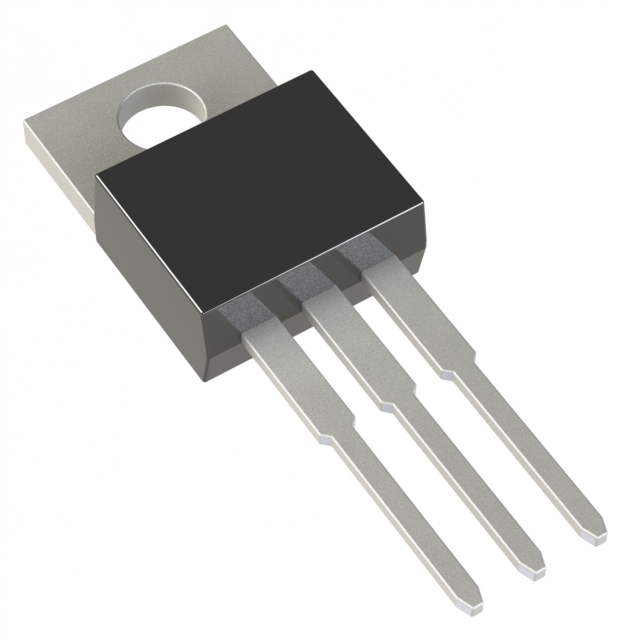
IXFP16N60P3 Equivalent & Substitute Parts
Part Overview
The IXFP16N60P3 is an N-Channel MOSFET manufactured by IXYS, rated for 600V drain-to-source voltage with 16A continuous drain current at 25°C. This device is part of the HiPerFET™ and Polar3™ series and is classified as Active product status. The component is housed in a TO-220-3 through-hole package and is suitable for high-voltage switching applications requiring robust thermal performance up to 347W at case temperature.
Substitute parts are necessary when the primary component becomes unavailable, when design requirements shift toward different current ratings or thermal characteristics, or when alternative manufacturers' components offer equivalent electrical performance within specified tolerances.
Substiute Parts
Key Parameters
| Parameter | Value | Unit |
|---|---|---|
| Drain to Source Voltage (Vdss) | 600 | V |
| Continuous Drain Current (Id) @ 25°C | 16 | A (Tc) |
| Drive Voltage (Max Rds On) | 10 | V |
| Rds On (Max) @ Id, Vgs | 470 | mOhm @ 500mA, 10V |
| Gate Charge (Qg) (Max) @ Vgs | 36 | nC @ 10V |
| Power Dissipation (Max) | 347 | W (Tc) |
| Operating Temperature Range | -55 to 150 | °C (TJ) |
| Package Type | TO-220-3 | Through Hole |
| FET Type | N-Channel | — |
| Technology | MOSFET (Metal Oxide) | — |
Substitute Part Grouping Explanation
Substitution eligibility for the IXFP16N60P3 is determined by the following critical parameters:
Mandatory Matching Criteria:
- Drain to Source Voltage (Vdss): 600V
- FET Type: N-Channel
- Technology: MOSFET (Metal Oxide)
- Package Type: TO-220-3 (through-hole mounting)
- Operating Temperature Range: -55°C to 150°C (TJ)
Flexible Parameters (Allow Variation):
- Continuous Drain Current (Id): Substitute parts may have lower current ratings if application requirements permit
- Power Dissipation (Max): Varies based on current rating and thermal design
- Rds On (Max): Acceptable within application-specific switching loss budgets
- Gate Charge (Qg): Acceptable within gate driver capability limits
The substitute parts listed below meet the mandatory matching criteria and are electrically compatible within the specified voltage and temperature operating envelope. Variations in current rating and power dissipation reflect different die designs and thermal characteristics from alternative manufacturers.
Parameter Comparison
| Parameter | IXFP16N60P3 | STP11N60DM2 | FCP7N60 |
|---|---|---|---|
| Manufacturer | IXYS | STMicroelectronics | onsemi |
| Drain to Source Voltage (Vdss) | 600V | 600V | 600V |
| Continuous Drain Current (Id) @ 25°C | 16A (Tc) | 10A (Tc) | 7A (Tc) |
| Drive Voltage (Max Rds On) | 10V | 10V | 10V |
| Rds On (Max) @ Id, Vgs | 470mOhm @ 500mA, 10V | 420mOhm @ 5A, 10V | 600mOhm @ 3.5A, 10V |
| Gate Charge (Qg) (Max) @ Vgs | 36nC @ 10V | 16.5nC @ 10V | 30nC @ 10V |
| Power Dissipation (Max) | 347W (Tc) | 110W (Tc) | 83W (Tc) |
| Operating Temperature Range | -55°C to 150°C (TJ) | -55°C to 150°C (TJ) | -55°C to 150°C (TJ) |
| Package Type | TO-220-3 | TO-220-3 | TO-220-3 |
| FET Type | N-Channel | N-Channel | N-Channel |
| Technology | MOSFET (Metal Oxide) | MOSFET (Metal Oxide) | MOSFET (Metal Oxide) |
| RoHS Status | ROHS3 Compliant | ROHS3 Compliant | ROHS3 Compliant |
| REACH Status | REACH Unaffected | REACH Unaffected | REACH Unaffected |
| Product Status | Active | Active | Not For New Designs |
Engineering Selection Recommendations
STP11N60DM2 (STMicroelectronics)
The STP11N60DM2 is the primary substitute for the IXFP16N60P3. This device maintains full voltage and temperature compatibility while offering 10A continuous drain current and 110W maximum power dissipation. The STP11N60DM2 carries Active product status, indicating ongoing manufacturer support and availability. It is ROHS3 compliant and REACH unaffected, meeting current regulatory requirements. The lower gate charge (16.5nC) compared to the IXFP16N60P3 (36nC) results in reduced gate drive power requirements. This substitute is suitable for applications where the 16A current rating of the primary part exceeds system requirements or where thermal management constraints limit power dissipation to 110W or below.
FCP7N60 (onsemi)
The FCP7N60 is a secondary substitute offering 7A continuous drain current and 83W maximum power dissipation. This device maintains full voltage and temperature compatibility with the IXFP16N60P3. However, the FCP7N60 carries Not For New Designs product status, indicating that onsemi does not recommend this component for new circuit development. While electrically compatible and currently in stock, the FCP7N60 should be selected only when existing designs require component replacement or when supply constraints on primary alternatives exist. ROHS3 compliance and REACH unaffected status are maintained.
Selection Criteria:
- For new designs requiring 600V, N-Channel MOSFET in TO-220-3 package: Select STP11N60DM2 (Active status, full support)
- For applications requiring current ratings below 10A: Select STP11N60DM2 or FCP7N60 based on thermal budget
- For existing designs currently using IXFP16N60P3: STP11N60DM2 provides direct substitution with improved gate charge characteristics
- All three devices operate across -55°C to 150°C temperature range and meet RoHS3 and REACH compliance requirements
Frequently Asked Questions (FAQ)
Q: Can the STP11N60DM2 directly replace the IXFP16N60P3 in existing designs?
A: The STP11N60DM2 is electrically compatible as a substitute. Both devices share identical 600V Vdss rating, N-Channel configuration, MOSFET technology, TO-220-3 package, and -55°C to 150°C operating temperature range. The primary difference is the continuous drain current rating (10A versus 16A). Direct substitution is valid for applications where the circuit current demand does not exceed 10A at 25°C case temperature. Gate charge differences (16.5nC versus 36nC) may improve gate driver efficiency but do not prevent substitution.
Q: Why does the FCP7N60 carry "Not For New Designs" status?
A: The FCP7N60 is classified as Not For New Designs by onsemi, indicating the manufacturer has discontinued active development and support for this component. While the device remains electrically compatible with the IXFP16N60P3 and is currently in inventory, onsemi recommends alternative components for new circuit development. This classification does not affect electrical performance or regulatory compliance but signals reduced long-term availability and manufacturer support.
Q: What is the significance of gate charge differences among these devices?
A: Gate charge (Qg) represents the total charge required to switch the MOSFET from off to on state. The IXFP16N60P3 requires 36nC at 10V, while the STP11N60DM2 requires only 16.5nC. Lower gate charge reduces the energy dissipated in the gate driver circuit and allows faster switching transitions. The FCP7N60 requires 30nC, intermediate between the other two. These differences do not prevent substitution but affect gate driver design and switching frequency capability.
Q: Are all three devices RoHS3 compliant and REACH unaffected?
A: Yes. The IXFP16N60P3, STP11N60DM2, and FCP7N60 are all ROHS3 compliant and REACH unaffected. All three devices meet current environmental and regulatory requirements for electronic component manufacturing and use in regulated markets.
Q: What thermal considerations apply when substituting these devices?
A: The IXFP16N60P3 is rated for 347W maximum power dissipation at case temperature, while the STP11N60DM2 is rated for 110W and the FCP7N60 for 83W. These differences reflect the continuous current ratings and on-resistance characteristics of each device. Thermal management requirements depend on application duty cycle, heatsink design, and ambient temperature. Applications requiring sustained power dissipation above 110W should retain the IXFP16N60P3 or verify that the substitute's thermal rating meets the specific application's power budget.
Q: Can these devices be used interchangeably in parallel configurations?
A: Parallel operation of different MOSFET models is not recommended without detailed analysis of current sharing characteristics, gate drive timing, and thermal management. While all three devices share the same voltage rating and package type, differences in Rds On characteristics and gate charge may result in unequal current distribution. Any parallel configuration requires verification of current balance and thermal performance specific to the application circuit.
Alternative Parts

SJ6012L2TP
Littelfuse Inc.
6 Alternative Parts

JMK107BBJ476MA-RE
Taiyo Yuden
10 Alternative Parts

GMK107BBJ475MA-T
Taiyo Yuden
5 Alternative Parts
SJ6020N2ARP
Littelfuse Inc.
3 Alternative Parts
SJ6025R2ATP
Littelfuse Inc.
4 Alternative Parts

2474-05L
API Delevan Inc.
1 Alternative Parts

4590R-684K
API Delevan Inc.
1 Alternative Parts

CM6560R-334
API Delevan Inc.
1 Alternative Parts

CM6460-104
API Delevan Inc.
1 Alternative Parts

5526-12
API Delevan Inc.
1 Alternative Parts