


Request Quote
(Ships tomorrow)
IXFN180N20 N-Channel MOSFET Equivalent & Substitute Parts
Part Overview
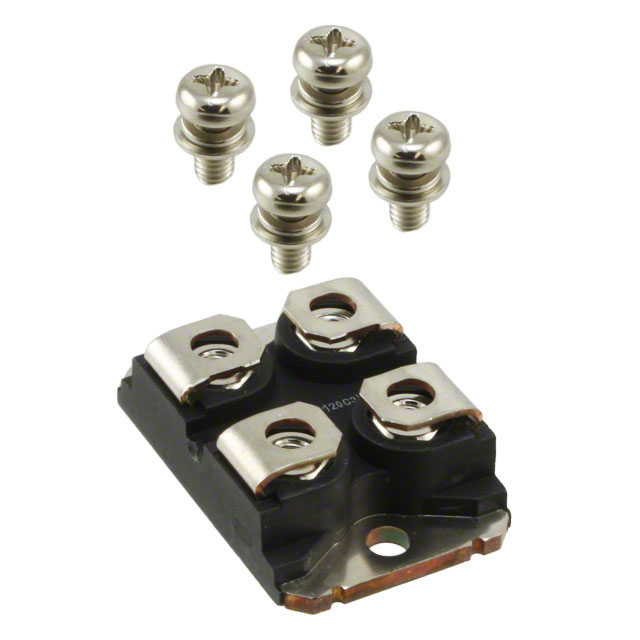
The IXFN180N20 is an N-Channel MOSFET rated for 200V drain-to-source voltage with 180A continuous drain current in a SOT-227B chassis mount package. This device is part of the IXYS HiPerFET™ series and is designated as "Not For New Designs," indicating it has been superseded in the manufacturer's product roadmap. Identification of equivalent and substitute parts is necessary for design continuity, inventory management, and long-term production support when the primary part becomes unavailable or when design requirements necessitate enhanced performance characteristics.
Substiute Parts
Key Parameters
| Parameter | Value | Unit |
|---|---|---|
| Drain-to-Source Voltage (Vdss) | 200 | V |
| Continuous Drain Current (Id) @ 25°C | 180 | A (Tc) |
| On-State Resistance (Rds On Max) @ Id, Vgs | 10 | mOhm @ 500mA, 10V |
| Gate Threshold Voltage (Vgs(th) Max) @ Id | 4 | V @ 8mA |
| Gate Charge (Qg Max) @ Vgs | 660 | nC @ 10V |
| Input Capacitance (Ciss Max) @ Vds | 22000 | pF @ 25V |
| Power Dissipation (Max) | 700 | W (Tc) |
| Operating Temperature Range | -55 to 150 | °C (TJ) |
| Package Type | SOT-227B (miniBLOC) | Chassis Mount |
| Series | HiPerFET™ | — |
Substitute Part Grouping Explanation
Substitution of the IXFN180N20 is determined by the following critical electrical and mechanical parameters:
Voltage Rating Compatibility: The substitute part must maintain the same 200V drain-to-source voltage (Vdss) rating to ensure circuit protection and reliability within the intended application voltage envelope.
Current Capacity: The substitute part must equal or exceed the 180A continuous drain current specification to support the same or higher load requirements without thermal derating.
On-State Resistance (Rds On): The substitute part's maximum on-state resistance must be compatible with the thermal and efficiency requirements of the application. Lower or equivalent Rds On values are acceptable as they reduce conduction losses.
Gate Charge (Qg): The substitute part's gate charge specification affects switching speed and driver circuit requirements. Compatibility is maintained when gate charge values are within acceptable ranges for the existing gate drive circuit.
Package and Mounting: The substitute part must use the same SOT-227B package and chassis mount configuration to ensure mechanical and thermal interface compatibility.
Operating Temperature Range: The substitute part must support the application's operating temperature requirements. Extended temperature ranges are acceptable.
The IXFN210N20P meets these substitution criteria while offering enhanced performance characteristics in power dissipation and current capacity.
Parameter Comparison
| Parameter | IXFN180N20 | IXFN210N20P | Unit |
|---|---|---|---|
| Manufacturer | IXYS | IXYS | — |
| FET Type | N-Channel | N-Channel | — |
| Technology | MOSFET (Metal Oxide) | MOSFET (Metal Oxide) | — |
| Drain-to-Source Voltage (Vdss) | 200 | 200 | V |
| Continuous Drain Current (Id) @ 25°C | 180 | 188 | A (Tc) |
| Drive Voltage (Max Rds On) | 10 | 10 | V |
| Rds On (Max) @ Id, Vgs | 10 | 10.5 | mOhm @ specified conditions |
| Vgs(th) (Max) @ Id | 4 | 4.5 | V @ 8mA |
| Gate Charge (Qg Max) @ Vgs | 660 | 255 | nC @ 10V |
| Vgs (Max) | ±20 | ±20 | V |
| Input Capacitance (Ciss Max) @ Vds | 22000 | 18600 | pF @ 25V |
| Power Dissipation (Max) | 700 | 1070 | W (Tc) |
| Operating Temperature Range | -55 to 150 | -55 to 175 | °C (TJ) |
| Mounting Type | Chassis Mount | Chassis Mount | — |
| Package / Case | SOT-227-4, miniBLOC | SOT-227-4, miniBLOC | — |
| Series | HiPerFET™ | HiPerFET™, Polar | — |
| RoHS Status | ROHS3 Compliant | ROHS3 Compliant | — |
| REACH Status | REACH Unaffected | REACH Unaffected | — |
| Product Status | Not For New Designs | Active | — |
Engineering Selection Recommendations
Primary Substitute: IXFN210N20P
The IXFN210N20P is the direct substitute for the IXFN180N20. Both devices share identical voltage ratings (200V Vdss), compatible current specifications (188A versus 180A), and identical package geometry (SOT-227B chassis mount). The IXFN210N20P is designated as an Active product, ensuring continued availability and manufacturer support.
Compliance and Certification Alignment:
Both the IXFN180N20 and IXFN210N20P maintain ROHS3 compliance and REACH Unaffected status, ensuring regulatory compatibility across applications. The substitute part's extended operating temperature range (-55°C to 175°C versus -55°C to 150°C) provides additional thermal margin for demanding applications.
Performance Enhancement:
The IXFN210N20P delivers superior power dissipation capability (1070W versus 700W), reduced gate charge (255 nC versus 660 nC), and lower input capacitance (18600 pF versus 22000 pF). These characteristics result in improved thermal performance, faster switching transitions, and reduced gate drive circuit stress.
Design Continuity:
Selection of the IXFN210N20P maintains mechanical and electrical interface compatibility with existing circuit designs while providing enhanced reliability through active product status and improved thermal characteristics.
Frequently Asked Questions (FAQ)
Q: Can the IXFN210N20P directly replace the IXFN180N20 in existing designs?
A: Yes. Both devices share identical 200V voltage ratings, compatible current specifications, and the same SOT-227B package configuration. No circuit modifications are required for mechanical or electrical interface compatibility.
Q: What is the significance of the IXFN180N20 being marked "Not For New Designs"?
A: This designation indicates the IXFN180N20 has been superseded in the manufacturer's product portfolio. While existing inventory remains available, IXYS recommends the IXFN210N20P for new design implementations to ensure long-term supply continuity and access to manufacturer technical support.
Q: How do the gate charge differences affect circuit performance?
A: The IXFN210N20P requires significantly less gate charge (255 nC versus 660 nC) to reach full conduction. This reduces the energy demand on the gate drive circuit, enabling faster switching transitions and lower driver power dissipation. Existing gate drive circuits designed for the IXFN180N20 will operate with improved performance margins when driving the IXFN210N20P.
Q: Are there thermal management differences between these devices?
A: The IXFN210N20P provides 53% higher maximum power dissipation (1070W versus 700W) and supports a 25°C higher maximum junction temperature (175°C versus 150°C). These characteristics enable improved thermal performance in high-current applications and provide additional design margin for thermal management.
Q: Do both devices require identical PCB layout and thermal interface considerations?
A: Yes. Both devices use the SOT-227B chassis mount package with identical mechanical dimensions and thermal interface requirements. Existing PCB designs and thermal management solutions are directly compatible with the substitute part.
Q: Are there any compliance or regulatory differences between the two parts?
A: No. Both the IXFN180N20 and IXFN210N20P maintain identical ROHS3 compliance and REACH Unaffected status. No regulatory or compliance modifications are required when implementing the substitute part.
Q: What is the input capacitance difference and does it affect circuit design?
A: The IXFN210N20P has lower input capacitance (18600 pF versus 22000 pF). This reduction improves high-frequency switching performance and reduces the capacitive load on the gate drive circuit, resulting in faster rise and fall times during switching transitions.
Alternative Parts

SJ6012L2TP
Littelfuse Inc.
6 Alternative Parts

JMK107BBJ476MA-RE
Taiyo Yuden
10 Alternative Parts

GMK107BBJ475MA-T
Taiyo Yuden
5 Alternative Parts
SJ6020N2ARP
Littelfuse Inc.
3 Alternative Parts
SJ6025R2ATP
Littelfuse Inc.
4 Alternative Parts

2474-05L
API Delevan Inc.
1 Alternative Parts

4590R-684K
API Delevan Inc.
1 Alternative Parts

CM6560R-334
API Delevan Inc.
1 Alternative Parts

CM6460-104
API Delevan Inc.
1 Alternative Parts

5526-12
API Delevan Inc.
1 Alternative Parts