


Request Quote
(Ships tomorrow)
IXFM67N10 Equivalent & Substitute Parts
Part Overview
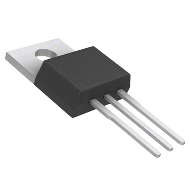
The IXFM67N10 is an N-Channel MOSFET manufactured by IXYS, rated for 100V drain-to-source voltage with 67A continuous drain current at 25°C. This device is housed in a TO-204AE through-hole package and is part of the HiPerFET™ series. The component is classified as obsolete, making identification of functionally equivalent alternatives necessary for ongoing design support, maintenance, and production continuity.
Substiute Parts
Key Parameters
| Parameter | Value | Unit |
|---|---|---|
| Drain-to-Source Voltage (Vdss) | 100 | V |
| Continuous Drain Current (Id) @ 25°C | 67 | A |
| On-State Resistance (Rds On Max) @ Id, Vgs | 25 mOhm @ 33.5A, 10V | mOhm |
| Gate Threshold Voltage (Vgs(th) Max) @ Id | 4 | V @ 4mA |
| Gate Charge (Qg Max) @ Vgs | 260 | nC @ 10V |
| Input Capacitance (Ciss Max) @ Vds | 4500 | pF @ 25V |
| Power Dissipation (Max) | 300 | W |
| Operating Temperature Range | -55 to 150 | °C |
| Package Type | TO-204AE | Through Hole |
| RoHS Status | ROHS3 Compliant | — |
Substitute Part Grouping Explanation
Substitution of the IXFM67N10 is determined by alignment of the following critical electrical and mechanical parameters:
Electrical Compatibility Criteria:
- Drain-to-Source Voltage (Vdss): Must equal or exceed 100V
- Continuous Drain Current (Id): Must equal or exceed 67A at 25°C
- Gate Threshold Voltage (Vgs(th)): Must be compatible at specified gate drive levels
- On-State Resistance (Rds On): Lower values indicate improved performance; higher values require thermal analysis
- Gate Charge (Qg): Lower values reduce switching losses; higher values increase gate drive requirements
- Input Capacitance (Ciss): Affects gate drive circuit design
Mechanical Compatibility Criteria:
- Package Type: Through-hole mounting required for direct board-level substitution
- Operating Temperature Range: Must support application thermal environment
Regulatory Compliance:
- RoHS3 Compliance: Required for environmental and supply chain standards
- REACH Status: Must maintain REACH Unaffected classification
The PSMN013-100PS,127 from Nexperia USA Inc. meets these substitution criteria with equivalent voltage rating, comparable current rating, and compatible through-hole packaging in TO-220AB format.
Parameter Comparison
| Parameter | IXFM67N10 (Main) | PSMN013-100PS,127 (Substitute) | Compatibility Notes |
|---|---|---|---|
| Manufacturer | IXYS | Nexperia USA Inc. | Different manufacturer; equivalent device class |
| Drain-to-Source Voltage (Vdss) | 100 V | 100 V | Identical |
| Continuous Drain Current (Id) @ 25°C | 67 A | 68 A | Substitute exceeds specification |
| On-State Resistance (Rds On Max) | 25 mOhm @ 33.5A, 10V | 13.9 mOhm @ 15A, 10V | Substitute exhibits lower resistance; improved thermal performance |
| Gate Threshold Voltage (Vgs(th) Max) | 4 V @ 4mA | 4 V @ 1mA | Equivalent threshold; substitute specified at lower current |
| Gate Charge (Qg Max) @ Vgs | 260 nC @ 10V | 59 nC @ 10V | Substitute requires significantly lower gate charge |
| Input Capacitance (Ciss Max) | 4500 pF @ 25V | 3195 pF @ 50V | Substitute exhibits lower input capacitance |
| Power Dissipation (Max) | 300 W | 170 W | Main part rated higher; substitute suitable for lower dissipation applications |
| Operating Temperature Range | -55 to 150 °C | -55 to 175 °C | Substitute supports extended upper temperature limit |
| Package Type | TO-204AE | TO-220AB | Different package footprint; both through-hole; board layout modification required |
| RoHS Status | ROHS3 Compliant | ROHS3 Compliant | Identical compliance |
| Product Status | Obsolete | Obsolete | Both components obsolete; long-term availability uncertain |
Engineering Selection Recommendations
Primary Consideration: Product Status
Both the IXFM67N10 and PSMN013-100PS,127 are classified as obsolete. This status indicates that neither component is in active production. Selection between these parts should prioritize current inventory availability and supply chain reliability.
Electrical Performance Assessment
The PSMN013-100PS,127 substitute meets the core voltage and current specifications of the IXFM67N10. The substitute exhibits superior on-state resistance characteristics (13.9 mOhm versus 25 mOhm), resulting in lower conduction losses and reduced thermal dissipation. Gate charge is substantially lower in the substitute (59 nC versus 260 nC), reducing gate drive circuit power requirements.
The main part is rated for higher maximum power dissipation (300W versus 170W). Applications requiring sustained high-power operation should evaluate thermal management implications when transitioning to the substitute.
Mechanical and Thermal Considerations
The IXFM67N10 uses TO-204AE packaging, while the PSMN013-100PS,127 uses TO-220AB packaging. These packages have different footprints and thermal characteristics. Board layout modification is required for direct substitution. The TO-220AB package may provide improved thermal coupling to heatsinks in certain mounting configurations.
Regulatory and Compliance Status
Both components maintain ROHS3 compliance and REACH Unaffected status, ensuring compatibility with current environmental and supply chain regulations. No compliance barriers exist for substitution.
Inventory and Availability
Current inventory records indicate 1,184 units of IXFM67N10 and 4,213 units of PSMN013-100PS,127 available as new original stock. The substitute part demonstrates higher current availability.
Frequently Asked Questions (FAQ)
Q: Can the PSMN013-100PS,127 directly replace the IXFM67N10 without circuit modification?
A: Electrical substitution is feasible based on voltage and current ratings. However, package footprint differences (TO-204AE versus TO-220AB) require board layout modification. Gate charge differences (59 nC versus 260 nC) may necessitate gate drive circuit adjustment to maintain switching performance.
Q: What is the impact of lower on-state resistance in the substitute part?
A: Lower on-state resistance (13.9 mOhm versus 25 mOhm) reduces conduction losses and heat generation. This improves overall circuit efficiency and may reduce thermal management requirements. Applications with high continuous current operation benefit from this characteristic.
Q: Why is the gate charge significantly lower in the substitute?
A: Gate charge is a function of device geometry and technology. The PSMN013-100PS,127 exhibits lower gate charge due to different internal structure. Lower gate charge reduces the energy required to switch the device and decreases gate drive circuit power dissipation. Gate drive circuits must be verified for compatibility with the lower charge requirement.
Q: Are there thermal management differences between the two packages?
A: TO-204AE and TO-220AB packages have different thermal characteristics. TO-220AB typically provides superior thermal coupling to external heatsinks due to its design. The main part (IXFM67N10) is rated for higher power dissipation (300W), suggesting it may be more suitable for high-power applications. Thermal analysis is required for specific application conditions.
Q: What is the significance of the extended operating temperature range in the substitute?
A: The PSMN013-100PS,127 supports operation to 175°C, compared to 150°C for the IXFM67N10. This extended range provides additional margin in high-temperature environments. Applications operating near the upper temperature limit of the main part may benefit from the substitute's extended rating.
Q: Are both parts suitable for new designs?
A: Both components are classified as obsolete and are not recommended for new designs. Obsolete status indicates discontinued production and uncertain long-term availability. New designs should evaluate current-generation MOSFET alternatives with equivalent electrical specifications and active production status.
Q: What packaging considerations apply to board redesign?
A: The TO-204AE package has a different pin configuration and footprint than TO-220AB. PCB layout, heatsink mounting, and thermal management strategies require redesign. Mechanical clearance around the device must be verified to accommodate the different package geometry.
Q: How do input capacitance differences affect circuit design?
A: Input capacitance (Ciss) affects gate drive circuit impedance and switching transient behavior. The substitute exhibits lower input capacitance (3195 pF versus 4500 pF), resulting in faster switching transitions and reduced gate drive circuit loading. Gate drive circuits designed for the main part operate within acceptable parameters with the substitute.
Alternative Parts

SJ6012L2TP
Littelfuse Inc.
6 Alternative Parts

JMK107BBJ476MA-RE
Taiyo Yuden
10 Alternative Parts

GMK107BBJ475MA-T
Taiyo Yuden
5 Alternative Parts
SJ6020N2ARP
Littelfuse Inc.
3 Alternative Parts
SJ6025R2ATP
Littelfuse Inc.
4 Alternative Parts

2474-05L
API Delevan Inc.
1 Alternative Parts

4590R-684K
API Delevan Inc.
1 Alternative Parts

CM6560R-334
API Delevan Inc.
1 Alternative Parts

CM6460-104
API Delevan Inc.
1 Alternative Parts

5526-12
API Delevan Inc.
1 Alternative Parts