


Request Quote
(Ships tomorrow)
IXFJ32N50Q Equivalent & Substitute Parts
Part Overview
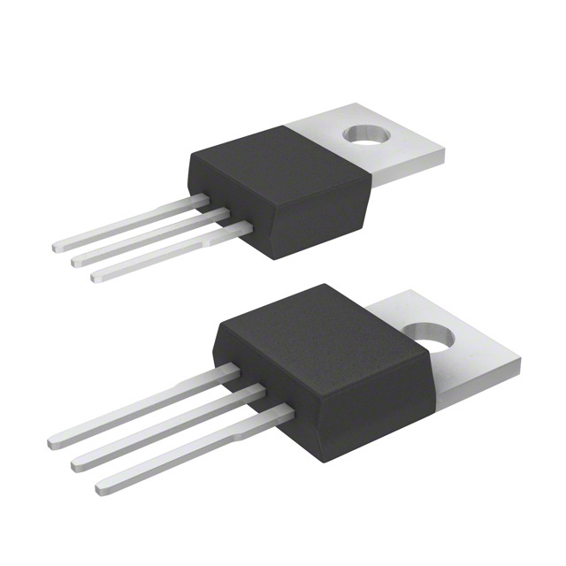
The IXFJ32N50Q is an N-Channel MOSFET manufactured by IXYS, rated for 500V drain-to-source voltage with 32A continuous drain current at 25°C. This device is part of the HiPerFET™ series and is housed in a TO-268 package for through-hole mounting applications. The part is currently listed as obsolete, necessitating identification of functionally equivalent alternatives for ongoing design support and procurement.
Substiute Parts
Key Parameters
| Parameter | Value | Unit |
|---|---|---|
| Drain to Source Voltage (Vdss) | 500 | V |
| Continuous Drain Current (Id) @ 25°C | 32 | A (Tc) |
| On-State Resistance (Rds On Max) @ 16A, 10V | 150 | mOhm |
| Gate Threshold Voltage (Vgs(th) Max) @ 4mA | 4 | V |
| Gate Charge (Qg Max) @ 10V | 153 | nC |
| Power Dissipation (Max) | 360 | W (Tc) |
| Operating Temperature Range | -55 to 150 | °C (TJ) |
| Package Type | TO-268 | Through Hole |
| FET Type | N-Channel | — |
| Technology | MOSFET (Metal Oxide) | — |
Substitute Part Grouping Explanation
Substitution of the IXFJ32N50Q is determined by the following electrical and mechanical criteria:
Primary Substitution Criteria:
- FET Type: N-Channel MOSFET
- Drain-to-Source Voltage (Vdss): Equal to or greater than 500V
- Continuous Drain Current (Id): Equal to or greater than 32A at 25°C
- On-State Resistance (Rds On): Lower or equivalent values preferred for thermal performance
- Gate Charge (Qg): Lower values reduce switching losses
- Operating Temperature Range: Minimum -55°C to 150°C
- Mounting Type: Through-hole configuration
Secondary Compatibility Factors:
- Package compatibility with TO-268 or TO-220-3 footprints
- Gate voltage ratings (Vgs Max) suitable for control circuitry
- Power dissipation capability meeting or exceeding application requirements
The IXFP34N65X2 qualifies as a substitute based on superior voltage rating (650V vs. 500V), higher current capability (34A vs. 32A), improved on-state resistance (105mOhm vs. 150mOhm), and higher power dissipation rating (540W vs. 360W). The substitute maintains N-Channel MOSFET topology, identical operating temperature range, and through-hole mounting configuration.
Parameter Comparison
| Parameter | IXFJ32N50Q | IXFP34N65X2 | Unit |
|---|---|---|---|
| Manufacturer | IXYS | IXYS | — |
| FET Type | N-Channel | N-Channel | — |
| Technology | MOSFET (Metal Oxide) | MOSFET (Metal Oxide) | — |
| Drain to Source Voltage (Vdss) | 500 | 650 | V |
| Continuous Drain Current (Id) @ 25°C | 32 | 34 | A (Tc) |
| Rds On (Max) @ Vgs 10V | 150 @ 16A | 105 @ 17A | mOhm |
| Gate Threshold Voltage (Vgs(th) Max) | 4 @ 4mA | 5.5 @ 2.5mA | V |
| Gate Charge (Qg Max) @ 10V | 153 | 56 | nC |
| Vgs (Max) | ±20 | ±30 | V |
| Input Capacitance (Ciss Max) @ 25V | 3950 | 3330 | pF |
| Power Dissipation (Max) | 360 | 540 | W (Tc) |
| Operating Temperature Range | -55 to 150 | -55 to 150 | °C (TJ) |
| Mounting Type | Through Hole | Through Hole | — |
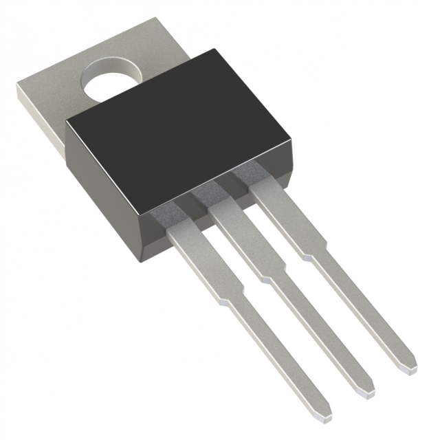
| Package Type | TO-268 | TO-220-3 | — |
| Product Status | Obsolete | Active | — |
| Series | HiPerFET™ | HiPerFET™, Ultra X2 | — |
Engineering Selection Recommendations
IXFP34N65X2 as Primary Substitute:
The IXFP34N65X2 is the recommended substitute for the obsolete IXFJ32N50Q based on the following engineering factors:
-
Product Status: The IXFP34N65X2 is listed as Active, ensuring long-term availability and supply chain continuity compared to the obsolete IXFJ32N50Q.
-
Electrical Performance Enhancement: The substitute provides superior electrical characteristics including higher voltage rating (650V vs. 500V), increased current capability (34A vs. 32A), reduced on-state resistance (105mOhm vs. 150mOhm), and significantly lower gate charge (56nC vs. 153nC), resulting in improved switching efficiency and reduced thermal dissipation.
-
Thermal Capability: Power dissipation rating increases from 360W to 540W, providing additional thermal margin for demanding applications.
-
Compliance and Certifications: The IXFP34N65X2 is RoHS3 Compliant, whereas the IXFJ32N50Q does not specify RoHS compliance. Both parts maintain REACH Unaffected status and EAR99 export classification.
-
Moisture Sensitivity: Both devices share identical MSL rating of 1 (Unlimited), indicating no moisture sensitivity concerns.
-
Package Consideration: The substitute uses TO-220-3 packaging instead of TO-268. Both are through-hole configurations; however, PCB layout modifications may be required to accommodate the different footprint geometry.
-
Gate Voltage Margin: The IXFP34N65X2 supports ±30V gate voltage compared to ±20V for the original part, providing additional design flexibility for gate drive circuits.
Frequently Asked Questions (FAQ)
Q: Can the IXFP34N65X2 directly replace the IXFJ32N50Q without circuit modifications?
A: The IXFP34N65X2 is electrically compatible as a substitute, meeting or exceeding all critical electrical parameters. However, PCB layout modifications are required due to different package types (TO-220-3 vs. TO-268). Gate drive circuits may require adjustment to accommodate the higher gate threshold voltage (5.5V vs. 4V) and different gate charge characteristics (56nC vs. 153nC).
Q: What are the key electrical advantages of the IXFP34N65X2 over the IXFJ32N50Q?
A: The substitute offers three primary advantages: (1) higher drain-to-source voltage rating (650V vs. 500V) provides increased design margin for overvoltage transients, (2) significantly reduced gate charge (56nC vs. 153nC) decreases switching losses and improves efficiency, and (3) lower on-state resistance (105mOhm vs. 150mOhm) reduces conduction losses and heat generation.
Q: Are there package compatibility concerns when substituting the IXFP34N65X2?
A: Yes. The IXFJ32N50Q uses TO-268 packaging while the IXFP34N65X2 uses TO-220-3 packaging. Both are through-hole configurations, but the physical dimensions and pin layouts differ. PCB footprint redesign is necessary. Verify thermal management requirements, as the different package geometries may affect heat dissipation characteristics.
Q: Does the IXFP34N65X2 require different gate drive voltage levels?
A: The IXFP34N65X2 has a higher gate threshold voltage (5.5V vs. 4V) and supports a wider gate voltage range (±30V vs. ±20V). Existing gate drive circuits designed for the IXFJ32N50Q may require adjustment to ensure adequate gate voltage margin and proper switching performance. Consult device datasheets for specific gate drive recommendations.
Q: What is the impact of the reduced gate charge on circuit performance?
A: The IXFP34N65X2 gate charge is 56nC compared to 153nC for the IXFJ32N50Q. Lower gate charge reduces the energy required to switch the device, resulting in lower switching losses, reduced heat generation, and improved overall circuit efficiency. Gate drive circuits may operate with lower current requirements.
Q: Is the IXFP34N65X2 suitable for applications requiring the original 500V rating?
A: Yes. The IXFP34N65X2 is rated for 650V, which exceeds the 500V requirement of the original application. The higher voltage rating provides additional design margin and protection against transient overvoltages without compromising performance in 500V applications.
Q: What compliance differences exist between the two parts?
A: The IXFP34N65X2 is RoHS3 Compliant, whereas the IXFJ32N50Q does not specify RoHS compliance status. Both parts are REACH Unaffected and classified as EAR99 for export purposes. If RoHS compliance is a design requirement, the IXFP34N65X2 is the appropriate choice.
Q: Are there thermal management differences between the TO-268 and TO-220-3 packages?
A: Both packages are through-hole configurations with different thermal characteristics. The TO-220-3 package used by the IXFP34N65X2 is widely supported by standard heatsink designs. Verify that existing heatsink mounting hardware is compatible with the TO-220-3 tab geometry. The higher power dissipation rating (540W vs. 360W) of the substitute may allow operation with reduced heatsink requirements.
Alternative Parts

SJ6012L2TP
Littelfuse Inc.
6 Alternative Parts

JMK107BBJ476MA-RE
Taiyo Yuden
10 Alternative Parts

GMK107BBJ475MA-T
Taiyo Yuden
5 Alternative Parts
SJ6020N2ARP
Littelfuse Inc.
3 Alternative Parts
SJ6025R2ATP
Littelfuse Inc.
4 Alternative Parts

2474-05L
API Delevan Inc.
1 Alternative Parts

4590R-684K
API Delevan Inc.
1 Alternative Parts

CM6560R-334
API Delevan Inc.
1 Alternative Parts

CM6460-104
API Delevan Inc.
1 Alternative Parts

5526-12
API Delevan Inc.
1 Alternative Parts