


Request Quote
(Ships tomorrow)
IXFH15N100Q3 Equivalent & Substitute Parts
Part Overview
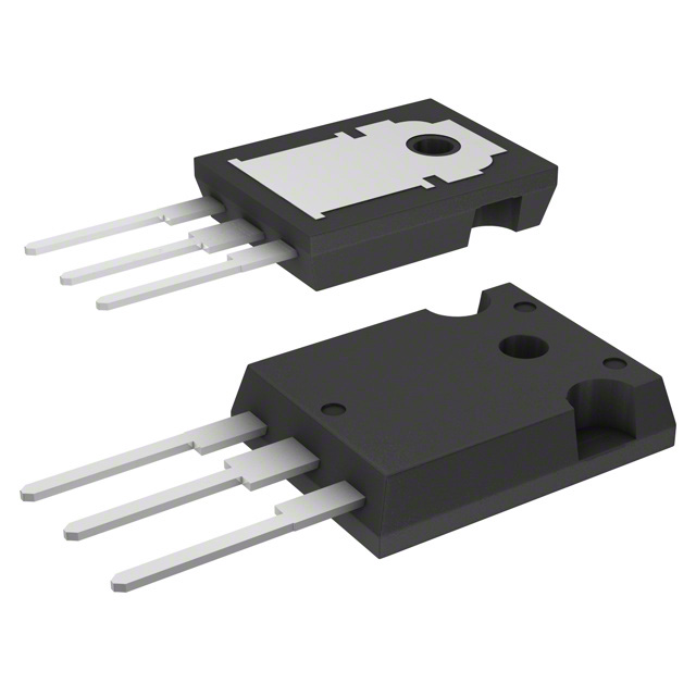
The IXFH15N100Q3 is an N-Channel MOSFET rated for 1000V drain-to-source voltage with 15A continuous drain current at 25°C. Manufactured by IXYS, this device belongs to the HiPerFET™ Q3 Class series and is housed in a TO-247AD through-hole package. The component is actively produced and RoHS3 compliant.
Substitute parts become necessary when the primary component experiences extended lead times, inventory constraints, or when system design parameters permit operation within the electrical and mechanical specifications of alternative devices. The substitute parts listed below maintain compatibility with the TO-247-3 package footprint and operate within the same temperature range.
Substiute Parts
Key Parameters
| Parameter | Value | Unit |
|---|---|---|
| Drain-to-Source Voltage (Vdss) | 1000 | V |
| Continuous Drain Current (Id) @ 25°C | 15 | A |
| On-State Resistance (Rds On Max) @ Id, Vgs | 1.05 | Ohm @ 7.5A, 10V |
| Gate Threshold Voltage (Vgs(th) Max) @ Id | 6.5 | V @ 4mA |
| Gate Charge (Qg Max) @ Vgs | 64 | nC @ 10V |
| Maximum Gate Voltage (Vgs Max) | ±30 | V |
| Input Capacitance (Ciss Max) @ Vds | 3250 | pF @ 25V |
| Power Dissipation (Max) | 690 | W |
| Operating Temperature Range | -55 to 150 | °C |
| Package Type | TO-247-3 | Through Hole |
| FET Technology | MOSFET (Metal Oxide) | N-Channel |
Substitute Part Grouping Explanation
Substitution eligibility for the IXFH15N100Q3 is determined by the following criteria:
Voltage Rating Compatibility: Substitute parts must have a Vdss rating equal to or greater than 1000V to maintain dielectric strength in the application circuit.
Current Rating Compatibility: Substitute parts must support continuous drain current (Id) at 25°C sufficient for the application. Reduced current ratings indicate lower power handling capability.
On-State Resistance (Rds On): Lower Rds On values reduce conduction losses and heat dissipation. Higher values increase power loss and thermal stress.
Gate Charge (Qg): Gate charge affects switching speed and driver circuit requirements. Variations in Qg influence gate drive energy and switching frequency performance.
Input Capacitance (Ciss): Input capacitance affects gate drive circuit design and switching transient behavior.
Power Dissipation Rating: Maximum power dissipation capability must align with thermal management requirements of the application.
Package and Mounting: All substitute parts must use TO-247-3 through-hole packaging to ensure mechanical and electrical compatibility with existing PCB layouts.
Temperature Range: All substitute parts operate across the -55°C to 150°C range, maintaining thermal compatibility.
Compliance Status: All parts maintain RoHS3 compliance, REACH unaffected status, and EAR99 export classification.
Parameter Comparison
| Parameter | IXFH15N100Q3 | STW11NK90Z | STW6N95K5 | Unit |
|---|---|---|---|---|
| Manufacturer | IXYS | STMicroelectronics | STMicroelectronics | — |
| Drain-to-Source Voltage (Vdss) | 1000 | 900 | 950 | V |
| Continuous Drain Current (Id) @ 25°C | 15 | 9.2 | 9 | A |
| Rds On (Max) @ Id, Vgs | 1.05 @ 7.5A, 10V | 0.98 @ 4.6A, 10V | 1.25 @ 3A, 10V | Ohm |
| Gate Threshold Voltage (Vgs(th) Max) @ Id | 6.5 @ 4mA | 4.5 @ 100µA | 5 @ 100µA | V |
| Gate Charge (Qg Max) @ Vgs | 64 @ 10V | 115 @ 10V | 13 @ 10V | nC |
| Maximum Gate Voltage (Vgs Max) | ±30 | ±30 | ±30 | V |
| Input Capacitance (Ciss Max) @ Vds | 3250 @ 25V | 3000 @ 25V | 450 @ 100V | pF |
| Power Dissipation (Max) | 690 | 200 | 90 | W |
| Operating Temperature Range | -55 to 150 | -55 to 150 | -55 to 150 | °C |
| Package Type | TO-247AD | TO-247-3 | TO-247-3 | — |
| Product Status | Active | Active | Active | — |
| RoHS Status | ROHS3 Compliant | ROHS3 Compliant | ROHS3 Compliant | — |
Engineering Selection Recommendations
IXFH15N100Q3 (Primary Component)
The IXFH15N100Q3 remains the preferred selection when full specifications are required. This device delivers 15A continuous drain current and 690W maximum power dissipation, supporting high-power applications. The 1000V Vdss rating provides maximum voltage margin. All three components maintain active product status and RoHS3 compliance.
STW11NK90Z (STMicroelectronics Substitute)
The STW11NK90Z operates at 900V Vdss and 9.2A continuous drain current. This substitute is suitable for applications where the voltage requirement does not exceed 900V and current demand does not exceed 9.2A. The device exhibits lower on-state resistance (0.98 Ohm) compared to the primary part, reducing conduction losses at the specified test point. However, maximum power dissipation is limited to 200W, restricting use in high-power thermal environments. Gate charge is elevated at 115 nC, requiring higher gate drive energy.
STW6N95K5 (STMicroelectronics Substitute)
The STW6N95K5 operates at 950V Vdss and 9A continuous drain current. This substitute is suitable for applications where voltage does not exceed 950V and current demand does not exceed 9A. The device exhibits significantly lower gate charge (13 nC) and input capacitance (450 pF @ 100V), enabling faster switching transients and reduced gate drive requirements. Maximum power dissipation is limited to 90W, restricting use to lower-power applications. On-state resistance is 1.25 Ohm at the specified test point.
All substitute parts are actively produced, RoHS3 compliant, and operate across the full -55°C to 150°C temperature range.
Frequently Asked Questions (FAQ)
Q: Can the STW11NK90Z replace the IXFH15N100Q3 in all applications?
A: The STW11NK90Z operates at reduced voltage (900V vs. 1000V) and current (9.2A vs. 15A) ratings. Substitution is valid only when the application circuit operates below 900V and requires less than 9.2A continuous drain current. The 200W power dissipation limit must also be verified against thermal requirements.
Q: What is the primary advantage of the STW6N95K5 substitute?
A: The STW6N95K5 exhibits significantly lower gate charge (13 nC vs. 64 nC) and input capacitance (450 pF vs. 3250 pF), enabling faster switching operation and reduced gate drive circuit complexity. This substitute is optimal for applications prioritizing switching speed over power handling capacity.
Q: Are all substitute parts compatible with existing PCB layouts designed for the IXFH15N100Q3?
A: The IXFH15N100Q3 uses TO-247AD packaging, while both substitute parts use TO-247-3 packaging. Both package types share the same three-pin through-hole footprint and pin configuration, ensuring mechanical and electrical compatibility with existing PCB designs.
Q: Do the substitute parts require different gate drive circuits?
A: The STW11NK90Z requires higher gate drive energy due to elevated gate charge (115 nC). The STW6N95K5 requires lower gate drive energy due to reduced gate charge (13 nC). Gate drive circuit adjustments may be necessary to optimize switching performance and minimize switching losses.
Q: What is the voltage derating consideration when using STW6N95K5?
A: The STW6N95K5 is rated for 950V Vdss, providing 50V less voltage margin than the primary IXFH15N100Q3 (1000V). Applications operating near maximum voltage must account for this reduced margin when evaluating circuit reliability and safety factors.
Q: Are all parts suitable for high-temperature operation?
A: All three parts operate across -55°C to 150°C. However, power dissipation ratings differ significantly. The IXFH15N100Q3 (690W) and STW11NK90Z (200W) support higher thermal loads than the STW6N95K5 (90W). Thermal management design must account for these differences.
Q: Do the substitute parts maintain the same compliance certifications?
A: All three parts are RoHS3 compliant, REACH unaffected, and classified as EAR99 for export purposes. Compliance status is equivalent across all devices.
Alternative Parts

SJ6012L2TP
Littelfuse Inc.
6 Alternative Parts

JMK107BBJ476MA-RE
Taiyo Yuden
10 Alternative Parts

GMK107BBJ475MA-T
Taiyo Yuden
5 Alternative Parts
SJ6020N2ARP
Littelfuse Inc.
3 Alternative Parts
SJ6025R2ATP
Littelfuse Inc.
4 Alternative Parts

2474-05L
API Delevan Inc.
1 Alternative Parts

4590R-684K
API Delevan Inc.
1 Alternative Parts

CM6560R-334
API Delevan Inc.
1 Alternative Parts

CM6460-104
API Delevan Inc.
1 Alternative Parts

5526-12
API Delevan Inc.
1 Alternative Parts