


Request Quote
(Ships tomorrow)
IXFC30N60P N-Channel 600V 15A MOSFET Equivalent & Substitute Parts
Part Overview
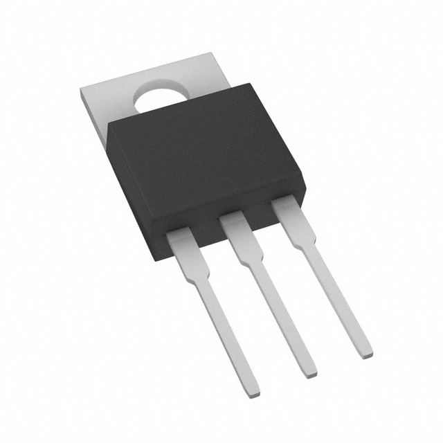
The IXFC30N60P is an N-Channel 600V 15A MOSFET manufactured by IXYS in the HiPerFET™ and PolarHT™ series. This device is rated for 166W power dissipation and features the ISOPLUS220™ through-hole package. The part is currently obsolete, making identification of equivalent and substitute components necessary for ongoing design support, maintenance, and production continuity.
Substitute parts listed in this reference maintain electrical compatibility within defined parameter ranges while offering alternative packaging options and active product status from current manufacturers.
Substiute Parts
Key Parameters
| Parameter | Value | Unit |
|---|---|---|
| FET Type | N-Channel | — |
| Drain to Source Voltage (Vdss) | 600 | V |
| Continuous Drain Current (Id) @ 25°C | 15 | A |
| Drive Voltage (Max Rds On) | 10 | V |
| Rds On (Max) @ Id, Vgs | 250 mOhm @ 15A, 10V | — |
| Gate Threshold Voltage Vgs(th) (Max) | 5 | V @ 4mA |
| Gate Charge (Qg) (Max) @ Vgs | 85 | nC @ 10V |
| Maximum Gate Voltage (Vgs) | ±30 | V |
| Input Capacitance (Ciss) (Max) @ Vds | 3820 | pF @ 25V |
| Power Dissipation (Max) | 166 | W |
| Operating Temperature Range | -55 to 150 | °C (TJ) |
| Mounting Type | Through Hole | — |
| Package | ISOPLUS220™ | — |
| Technology | MOSFET (Metal Oxide) | — |
| Moisture Sensitivity Level (MSL) | 1 (Unlimited) | — |
| REACH Status | REACH Unaffected | — |
Substitute Part Grouping Explanation
Substitution of the IXFC30N60P is determined by the following critical electrical and mechanical parameters:
Primary Matching Criteria:
- Drain to Source Voltage (Vdss): 600V nominal (560V–650V acceptable range)
- Continuous Drain Current (Id): 15A minimum at 25°C
- Drive Voltage: 10V gate drive capability
- Gate Threshold Voltage: Compatible with standard gate drive circuits (3.8V–5V range)
- Operating Temperature: -55°C to 150°C minimum
- Mounting: Through-hole configuration required
- Technology: N-Channel MOSFET (Metal Oxide)
Secondary Considerations:
- Rds On (Max): Values between 250–290 mOhm at rated conditions maintain performance equivalence
- Gate Charge (Qg): Lower values (15.6–85 nC) indicate improved switching characteristics
- Input Capacitance (Ciss): Variations reflect different die designs but do not affect substitution eligibility
- Power Dissipation: Higher ratings provide thermal margin; lower ratings require thermal design verification
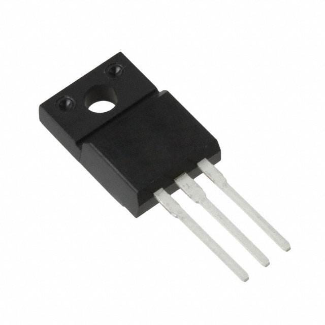
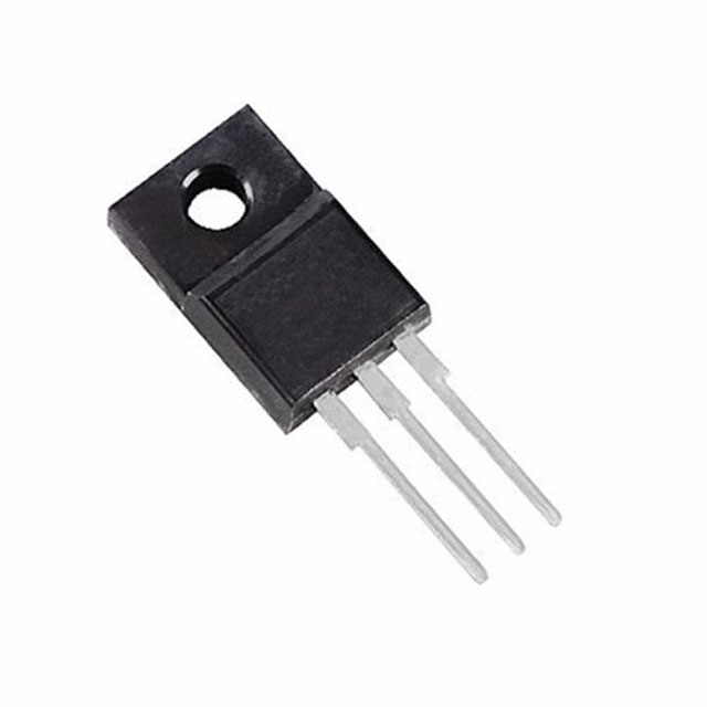
- Package Format: ISOPLUS220™, TO-220AB, TO-220FM, TO-220-3, and TO-247 packages are mechanically compatible in through-hole applications
Substitute parts meeting these criteria are grouped by package type and active product status.
Parameter Comparison
| Parameter | IXFC30N60P | SIHP15N60E-GE3 | AOTF15S60L | R6015ENX | R6015KNX | R6020FNX | APT15F60B | SPA15N60C3XKSA1 | SPA16N50C3XKSA1 | STF18N60M2 | STF18NM60N |
|---|---|---|---|---|---|---|---|---|---|---|---|
| Vdss (V) | 600 | 600 | 600 | 600 | 600 | 600 | 600 | 650 | 560 | 600 | 600 |
| Id @ 25°C (A) | 15 | 15 | 15 | 15 | 15 | 20 | 16 | 15 | 16 | 13 | 13 |
| Rds On (Max) mOhm | 250 @ 15A, 10V | 280 @ 8A, 10V | 290 @ 7.5A, 10V | 290 @ 6.5A, 10V | 290 @ 6.5A, 10V | 250 @ 10A, 10V | 430 @ 7A, 10V | 280 @ 9.4A, 10V | 280 @ 10A, 10V | 280 @ 6.5A, 10V | 285 @ 6.5A, 10V |
| Vgs(th) (Max) (V) | 5 @ 4mA | 4 @ 250µA | 3.8 @ 250µA | 4 @ 1mA | 5 @ 1mA | 5 @ 1mA | 5 @ 500µA | 3.9 @ 675µA | 3.9 @ 675µA | 4 @ 250µA | 4 @ 250µA |
| Qg (Max) (nC) | 85 @ 10V | 78 @ 10V | 15.6 @ 10V | 40 @ 10V | 27.5 @ 10V | 65 @ 10V | 72 @ 10V | 63 @ 10V | 66 @ 10V | 21.5 @ 10V | 35 @ 10V |
| Ciss (Max) (pF) | 3820 @ 25V | 1350 @ 100V | 717 @ 100V | 910 @ 25V | 1050 @ 25V | 2040 @ 25V | 2882 @ 25V | 1660 @ 25V | 1600 @ 25V | 791 @ 100V | 1000 @ 50V |
| Vgs (Max) (V) | ±30 | ±30 | ±30 | ±20 | ±20 | ±30 | ±30 | ±20 | ±20 | ±25 | ±25 |
| Power Dissipation (Max) (W) | 166 | 180 | 27.8 | 40 | 60 | 50 | 290 | 34 | 34 | 25 | 30 |
| Operating Temp (°C) | -55 to 150 | -55 to 150 | -55 to 150 | -55 to 150 | -55 to 150 | -55 to 150 | -55 to 150 | -55 to 150 | -55 to 150 | -55 to 150 | -55 to 150 |
| Package | ISOPLUS220™ | TO-220AB | TO-220-3F | TO-220FM | TO-220FM | TO-220FM | TO-247-3 | TO-220-3 FP | TO-220-3 FP | TO-220FP | TO-220FP |
| Product Status | Obsolete | Active | Active | Active | Active | Active | Active | Active | Last Time Buy | Active | Active |
| RoHS Status | — | ROHS3 Compliant | — | ROHS3 Compliant | ROHS3 Compliant | ROHS3 Compliant | ROHS3 Compliant | ROHS3 Compliant | ROHS3 Compliant | ROHS3 Compliant | ROHS3 Compliant |
Engineering Selection Recommendations
Primary Substitutes (Highest Compatibility):
The following parts are recommended as direct substitutes based on electrical parameter alignment and active product status:
-
SIHP15N60E-GE3 (Vishay Siliconix): Active product with 600V/15A rating, 180W power dissipation, TO-220AB package. Gate charge of 78 nC closely matches the original 85 nC specification. ROHS3 compliant.
-
R6015KNX (Rohm Semiconductor): Active product with 600V/15A rating, 60W power dissipation, TO-220FM package. Gate charge of 27.5 nC provides improved switching performance. ROHS3 compliant with full -55°C to 150°C temperature range.
-
STF18N60M2 (STMicroelectronics): Active product with 600V/13A rating, 25W power dissipation, TO-220FP package. Lower gate charge (21.5 nC) and input capacitance reduce switching losses. ROHS3 compliant.
Secondary Substitutes (Parameter Trade-offs):
-
AOTF15S60L (Alpha & Omega Semiconductor): Active product with 600V/15A rating, 27.8W power dissipation, TO-220-3F package. Significantly lower power dissipation requires thermal design verification in high-power applications.
-
R6020FNX (Rohm Semiconductor): Active product with 600V/20A rating, 50W power dissipation, TO-220FM package. Higher current rating provides design margin but requires PCB layout verification for thermal management.
-
APT15F60B (Microsemi Corporation): Active product with 600V/16A rating, 290W power dissipation, TO-247-3 package. Highest power dissipation rating suitable for demanding thermal environments.
Voltage-Variant Substitutes:
-
SPA15N60C3XKSA1 (Infineon Technologies): Active product with 650V/15A rating, 34W power dissipation, TO-220-3 FP package. Higher voltage rating provides overvoltage margin. ROHS3 compliant.
-
SPA16N50C3XKSA1 (Infineon Technologies): Last Time Buy status with 560V/16A rating, 34W power dissipation, TO-220-3 FP package. Lower voltage rating suitable for applications with reduced voltage stress.
Compliance and Certification:
All recommended substitutes maintain REACH Unaffected status and EAR99 export classification consistent with the original IXFC30N60P. Moisture Sensitivity Level 1 (Unlimited) is maintained across all alternatives, eliminating special handling requirements.
Frequently Asked Questions (FAQ)
Q: Can the IXFC30N60P be directly replaced with any of these substitutes without PCB modification?
A: Direct replacement depends on package compatibility. The original ISOPLUS220™ package is specific to IXYS. Substitutes in TO-220AB, TO-220FM, TO-220-3F, and TO-220FP packages are mechanically compatible with standard through-hole PCB layouts. The TO-247-3 package (APT15F60B) requires different PCB footprint and mounting hardware. Verify PCB hole spacing and lead configuration before substitution.
Q: What is the significance of the gate charge (Qg) differences between the original and substitute parts?
A: Gate charge determines the energy required to switch the MOSFET on and off. The original IXFC30N60P specifies 85 nC at 10V. Substitutes with lower gate charge (15.6–40 nC) reduce switching losses and allow faster switching speeds, improving efficiency in high-frequency applications. Substitutes with similar gate charge (78–85 nC) maintain equivalent switching behavior. Gate drive circuits must supply sufficient current to charge the gate within the required switching time.
Q: Are there thermal considerations when substituting parts with different power dissipation ratings?
A: Yes. The original IXFC30N60P is rated for 166W power dissipation. Substitutes with lower ratings (25–60W) dissipate less heat under identical operating conditions, reducing thermal stress on the device but requiring verification that junction temperature remains within limits. Substitutes with higher ratings (180–290W) provide thermal margin and are suitable for applications approaching the original power dissipation limit. Thermal design must account for actual power loss, which depends on switching frequency, duty cycle, and load current.
Q: What is the impact of Rds On (on-state resistance) variations on circuit performance?
A: Rds On determines conduction losses when the MOSFET is in the on-state. The original IXFC30N60P specifies 250 mOhm at 15A and 10V gate drive. Substitutes with similar Rds On (280–290 mOhm) produce equivalent conduction losses. Higher Rds On values (430 mOhm in APT15F60B) increase conduction losses and heat generation. Lower Rds On values improve efficiency. Rds On is temperature-dependent and increases at elevated junction temperatures, affecting circuit performance in thermal stress conditions.
Q: Can substitutes with different drain current ratings (13A, 16A, 20A) be used in 15A applications?
A: Yes, with design considerations. Substitutes rated for higher continuous drain current (16A, 20A) provide current margin and are directly compatible. Substitutes rated for lower continuous drain current (13A in STF18N60M2, STF18NM60N) require verification that actual circuit current does not exceed the device rating. Lower-rated devices may reach thermal limits faster under sustained high-current operation. Current derating curves in device datasheets must be consulted for applications operating near maximum ratings.
Q: What is the difference between TO-220AB, TO-220FM, TO-220-3F, and TO-220FP package variants?
A: All variants are through-hole TO-220 family packages with three leads (Gate, Drain, Source) and compatible PCB footprints. TO-220AB is the standard variant. TO-220FM and TO-220FP include full-pack isolation features. TO-220-3F indicates a full-pack configuration. Mechanical compatibility is maintained across variants for standard through-hole PCB designs. Verify lead spacing and mounting hole diameter with PCB design files before production.
Q: How do gate threshold voltage (Vgs(th)) differences affect gate drive circuit design?
A: Gate threshold voltage determines the minimum gate-source voltage required to turn the MOSFET on. The original IXFC30N60P specifies 5V at 4mA. Substitutes range from 3.8V to 5V at various test currents. Lower threshold voltages (3.8–3.9V) allow operation with lower gate drive voltages, reducing gate drive power consumption. Higher threshold voltages (5V) require higher gate drive voltages for full on-state conduction. Standard 10V gate drive circuits are compatible with all listed substitutes. Verify gate drive voltage supply capability and circuit timing margins for applications using marginal gate drive voltages.
Q: What does "Last Time Buy" status mean for SPA16N50C3XKSA1?
A: Last Time Buy status indicates that the manufacturer has announced end-of-life for this product. Existing inventory may be available for a limited time, but the part will not be manufactured indefinitely. For new designs or long-term production, select substitutes with Active product status (SIHP15N60E-GE3, R6015KNX, STF18N60M2, AOTF15S60L, R6020FNX, APT15F60B, SPA15N60C3XKSA1, STF18NM60N) to ensure supply continuity.
Q: Are all substitutes ROHS3 compliant?
A: All listed substitutes are ROHS3 compliant. The original IXFC30N60P does not specify RoHS status due to its obsolete status. ROHS3 compliance ensures that substitutes meet current environmental regulations for lead-free manufacturing and restricted hazardous substances, supporting compliance with EU directives and customer requirements.
Q: Can input capacitance (Ciss) differences affect circuit performance?
A: Input capacitance affects gate charge requirements and switching speed. The original IXFC30N60P specifies 3820 pF at 25V. Substitutes range from 717 pF to 2882 pF. Lower input capacitance reduces gate charge and switching losses, improving efficiency in high-frequency applications. Higher input capacitance increases gate charge and switching time. Gate drive circuits with sufficient current capability accommodate these variations. For applications with marginal gate drive current, lower-capacitance substitutes (AOTF15S60L at 717 pF) reduce gate drive stress.
Alternative Parts

SJ6012L2TP
Littelfuse Inc.
6 Alternative Parts

JMK107BBJ476MA-RE
Taiyo Yuden
10 Alternative Parts

GMK107BBJ475MA-T
Taiyo Yuden
5 Alternative Parts
SJ6020N2ARP
Littelfuse Inc.
3 Alternative Parts
SJ6025R2ATP
Littelfuse Inc.
4 Alternative Parts

2474-05L
API Delevan Inc.
1 Alternative Parts

4590R-684K
API Delevan Inc.
1 Alternative Parts

CM6560R-334
API Delevan Inc.
1 Alternative Parts

CM6460-104
API Delevan Inc.
1 Alternative Parts

5526-12
API Delevan Inc.
1 Alternative Parts