


Request Quote
(Ships tomorrow)
IS25LQ032B-JBLE Equivalent & Substitute Parts
Part Overview
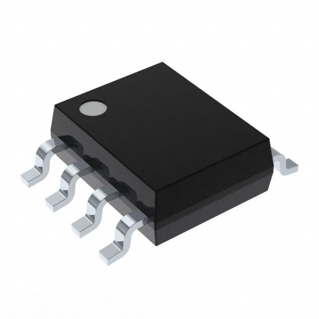
The IS25LQ032B-JBLE is a 32Mbit NOR Flash memory IC with SPI Quad I/O interface, manufactured by ISSI (Integrated Silicon Solution Inc). This device operates at 104 MHz clock frequency and is housed in an 8-SOIC surface mount package. The part is currently classified as obsolete, making identification of compatible substitute components essential for ongoing system support and new design implementations. Substitute parts must maintain electrical and mechanical compatibility while meeting the same functional requirements for NOR Flash memory applications.
Substiute Parts
Key Parameters
| Parameter | Value |
|---|---|
| Memory Size | 32Mbit |
| Memory Format | FLASH - NOR |
| Memory Interface | SPI - Quad I/O |
| Clock Frequency | 104 MHz |
| Memory Organization | 4M x 8 |
| Voltage Supply Range | 2.3V ~ 3.6V |
| Operating Temperature | -40°C ~ 105°C (TA) |
| Package Type | 8-SOIC (0.209", 5.30mm Width) |
| Write Cycle Time | 1ms |
| RoHS Status | ROHS3 Compliant |
| MSL Rating | 3 (168 Hours) |
Substitute Part Grouping Explanation
Substitution eligibility for the IS25LQ032B-JBLE is determined by the following critical parameters:
Memory Capacity & Organization: Substitute parts must provide 32Mbit capacity with 4M x 8 organization to ensure direct functional equivalence in memory addressing and data storage.
Memory Technology & Interface: The NOR Flash technology with SPI Quad I/O interface is mandatory. Substitute parts must support the same quad I/O communication protocol for signal compatibility with existing PCB designs and firmware implementations.
Electrical Specifications: Supply voltage range of 2.3V ~ 3.6V and operating temperature range of -40°C ~ 105°C must be maintained to ensure operation within the same system power and thermal constraints.
Package Compatibility: The 8-SOIC package with 0.209" (5.30mm) width is required for mechanical fit on existing PCBs. Pin count and pitch must remain identical.
Compliance & Certifications: RoHS3 compliance and MSL rating of 3 (168 Hours) must be preserved for regulatory and manufacturing process compatibility.
The IS25LP032D-JBLE meets all substitution criteria while offering enhanced performance characteristics.
Parameter Comparison
| Parameter | IS25LQ032B-JBLE (Main Part) | IS25LP032D-JBLE (Substitute) |
|---|---|---|
| Manufacturer | ISSI | Integrated Silicon Solution |
| Memory Size | 32Mbit | 32Mbit |
| Memory Format | FLASH - NOR | FLASH - NOR |
| Memory Organization | 4M x 8 | 4M x 8 |
| Memory Interface | SPI - Quad I/O | SPI - Quad I/O, QPI, DTR |
| Clock Frequency | 104 MHz | 133 MHz |
| Write Cycle Time | 1ms | 800µs |
| Voltage Supply Range | 2.3V ~ 3.6V | 2.3V ~ 3.6V |
| Operating Temperature | -40°C ~ 105°C (TA) | -40°C ~ 105°C (TA) |
| Package Type | 8-SOIC (0.209", 5.30mm Width) | 8-SOIC (0.209", 5.30mm Width) |
| RoHS Status | ROHS3 Compliant | ROHS3 Compliant |
| MSL Rating | 3 (168 Hours) | 3 (168 Hours) |
| Product Status | Obsolete | Active |
Engineering Selection Recommendations
The IS25LP032D-JBLE is a direct substitute for the IS25LQ032B-JBLE based on matching memory capacity, organization, interface protocol, electrical specifications, and package geometry. Both parts maintain identical supply voltage ranges (2.3V ~ 3.6V) and operating temperature specifications (-40°C ~ 105°C), ensuring compatibility with existing system designs.
The substitute part offers enhanced performance through increased clock frequency (133 MHz versus 104 MHz) and reduced write cycle time (800µs versus 1ms), providing operational improvements without compromising backward compatibility. Both parts maintain ROHS3 compliance and identical MSL ratings, satisfying regulatory and manufacturing requirements.
The IS25LP032D-JBLE is currently in active production status, ensuring long-term availability and supply chain stability compared to the obsolete IS25LQ032B-JBLE.
Frequently Asked Questions (FAQ)
Q: Can the IS25LP032D-JBLE be used as a direct replacement for the IS25LQ032B-JBLE?
A: Yes. Both parts share identical memory capacity (32Mbit), organization (4M x 8), NOR Flash technology, SPI Quad I/O interface, supply voltage range (2.3V ~ 3.6V), operating temperature range (-40°C ~ 105°C), and 8-SOIC package dimensions. Pin-to-pin compatibility is maintained.
Q: What are the performance differences between these parts?
A: The IS25LP032D-JBLE operates at 133 MHz clock frequency compared to 104 MHz for the IS25LQ032B-JBLE. Write cycle time is reduced from 1ms to 800µs. The substitute part also supports additional interface modes (QPI and DTR) beyond the standard SPI Quad I/O. These enhancements do not affect backward compatibility.
Q: Are there any firmware or software modifications required when switching to the IS25LP032D-JBLE?
A: No firmware modifications are required. The substitute part maintains full compatibility with the SPI Quad I/O protocol used by the original part. Existing firmware will operate without changes.
Q: Do both parts meet the same compliance standards?
A: Yes. Both the IS25LQ032B-JBLE and IS25LP032D-JBLE are ROHS3 compliant with MSL rating 3 (168 Hours). Regulatory and manufacturing process requirements are identical.
Q: Why is the IS25LQ032B-JBLE listed as obsolete?
A: The IS25LQ032B-JBLE has reached end-of-life status. The IS25LP032D-JBLE represents the current active production equivalent from the same manufacturer, ensuring continued availability and support.
Q: Are there any thermal or power consumption differences?
A: Both parts operate within the same voltage supply range (2.3V ~ 3.6V) and temperature specifications (-40°C ~ 105°C). The enhanced performance of the substitute part may result in different power consumption characteristics under specific operating conditions, but both are suitable for the same system power budgets.
Alternative Parts

SJ6012L2TP
Littelfuse Inc.
6 Alternative Parts

JMK107BBJ476MA-RE
Taiyo Yuden
10 Alternative Parts

GMK107BBJ475MA-T
Taiyo Yuden
5 Alternative Parts
SJ6020N2ARP
Littelfuse Inc.
3 Alternative Parts
SJ6025R2ATP
Littelfuse Inc.
4 Alternative Parts

2474-05L
API Delevan Inc.
1 Alternative Parts

4590R-684K
API Delevan Inc.
1 Alternative Parts

CM6560R-334
API Delevan Inc.
1 Alternative Parts

CM6460-104
API Delevan Inc.
1 Alternative Parts

5526-12
API Delevan Inc.
1 Alternative Parts