


Request Quote
(Ships tomorrow)
IS25LD040-JBLE Equivalent & Substitute Parts
Part Overview
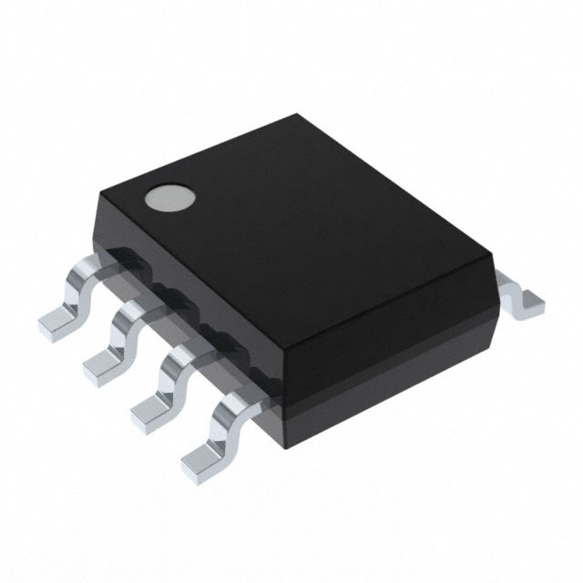
The IS25LD040-JBLE is a 4Mbit SPI FLASH memory IC manufactured by ISSI (Integrated Silicon Solution Inc) in an 8-SOIC surface mount package. This device operates at 100 MHz clock frequency with a supply voltage range of 2.3V to 3.6V and supports temperatures from -40°C to 105°C. The part is classified as obsolete, making equivalent substitutes necessary for ongoing production and maintenance applications requiring 4Mbit SPI FLASH memory functionality.
Substiute Parts
Key Parameters
| Parameter | Value |
|---|---|
| Memory Size | 4Mbit |
| Memory Format | FLASH |
| Memory Interface | SPI |
| Memory Organization | 512K x 8 |
| Clock Frequency | 100 MHz |
| Voltage Supply Range | 2.3V ~ 3.6V |
| Operating Temperature | -40°C ~ 105°C |
| Package Type | 8-SOIC (0.209", 5.30mm Width) |
| Write Cycle Time | 5ms |
| RoHS Status | ROHS3 Compliant |
| Moisture Sensitivity Level | 3 (168 Hours) |
Substitute Part Grouping Explanation
Substitution for the IS25LD040-JBLE is based on the following critical parameters that must remain compatible:
- Memory capacity: 4Mbit (512K x 8 organization)
- Interface protocol: SPI
- Package format: 8-SOIC with identical 5.30mm width
- Supply voltage overlap: Minimum 2.3V to 3.6V range
- Non-volatile FLASH memory technology
- RoHS3 compliance and MSL 3 rating
The SST25VF040B-50-4I-S2AF-T meets these core substitution criteria. While it operates at 50 MHz (lower than the original 100 MHz specification) and supports a narrower voltage range (2.7V ~ 3.6V), it maintains identical memory capacity, organization, SPI interface, and 8-SOIC packaging. The write cycle time difference (10µs vs 5ms) reflects different measurement methodologies for the same functional capability.
Parameter Comparison
| Parameter | IS25LD040-JBLE | SST25VF040B-50-4I-S2AF-T |
|---|---|---|
| Manufacturer | ISSI | Microchip Technology |
| Memory Size | 4Mbit | 4Mbit |
| Memory Organization | 512K x 8 | 512K x 8 |
| Memory Interface | SPI | SPI |
| Clock Frequency | 100 MHz | 50 MHz |
| Voltage Supply Range | 2.3V ~ 3.6V | 2.7V ~ 3.6V |
| Operating Temperature | -40°C ~ 105°C | -40°C ~ 85°C |
| Package / Case | 8-SOIC (0.209", 5.30mm Width) | 8-SOIC (0.209", 5.30mm Width) |
| Product Status | Obsolete | Active |
| RoHS Status | ROHS3 Compliant | ROHS3 Compliant |
| Moisture Sensitivity Level | 3 (168 Hours) | 3 (168 Hours) |
Engineering Selection Recommendations
The SST25VF040B-50-4I-S2AF-T is the qualified substitute for IS25LD040-JBLE applications. Selection should be based on the following factors:
- The substitute maintains identical memory capacity and SPI interface protocol, ensuring functional compatibility at the firmware level
- Both devices are ROHS3 compliant with matching MSL 3 ratings, supporting equivalent supply chain and storage requirements
- The substitute is in active production status, providing long-term availability and supply continuity
- Clock frequency reduction from 100 MHz to 50 MHz is acceptable for applications where the original 100 MHz specification was not a critical performance requirement
- The narrower operating temperature range (-40°C to 85°C vs -40°C to 105°C) must be evaluated against specific application thermal requirements
- The minimum supply voltage requirement increases from 2.3V to 2.7V; applications operating below 2.7V require alternative solutions
- Identical 8-SOIC packaging enables direct PCB footprint compatibility without layout modifications
Frequently Asked Questions (FAQ)
Q: Can SST25VF040B-50-4I-S2AF-T replace IS25LD040-JBLE in all applications?
A: The substitute is compatible for applications where the 50 MHz clock frequency meets performance requirements and the operating temperature range does not exceed 85°C. Applications requiring operation below 2.7V supply voltage or above 85°C require alternative solutions.
Q: What is the difference between the 100 MHz and 50 MHz clock frequencies?
A: Clock frequency determines the maximum data transfer rate. The 50 MHz substitute supports lower throughput than the 100 MHz original. Compatibility depends on whether the application's data transfer requirements can be met at 50 MHz.
Q: Are the packages physically identical?
A: Both devices use 8-SOIC packaging with 0.209" (5.30mm) width. PCB footprints are identical, allowing direct component substitution without layout changes.
Q: Do both parts meet the same compliance standards?
A: Both IS25LD040-JBLE and SST25VF040B-50-4I-S2AF-T are ROHS3 compliant with MSL 3 moisture sensitivity ratings. Compliance requirements are equivalent.
Q: What is the impact of the voltage supply range difference?
A: The original part operates from 2.3V to 3.6V, while the substitute operates from 2.7V to 3.6V. Applications using supply voltages between 2.3V and 2.7V cannot use the substitute without additional voltage regulation.
Q: Is the substitute available in the same packaging format?
A: The SST25VF040B-50-4I-S2AF-T is supplied in Tape & Reel (TR) format, while the original part packaging format was not specified. Both use identical 8-SOIC case dimensions for PCB compatibility.
Alternative Parts

SJ6012L2TP
Littelfuse Inc.
6 Alternative Parts

JMK107BBJ476MA-RE
Taiyo Yuden
10 Alternative Parts

GMK107BBJ475MA-T
Taiyo Yuden
5 Alternative Parts
SJ6020N2ARP
Littelfuse Inc.
3 Alternative Parts
SJ6025R2ATP
Littelfuse Inc.
4 Alternative Parts

2474-05L
API Delevan Inc.
1 Alternative Parts

4590R-684K
API Delevan Inc.
1 Alternative Parts

CM6560R-334
API Delevan Inc.
1 Alternative Parts

CM6460-104
API Delevan Inc.
1 Alternative Parts

5526-12
API Delevan Inc.
1 Alternative Parts