


Request Quote
(Ships tomorrow)
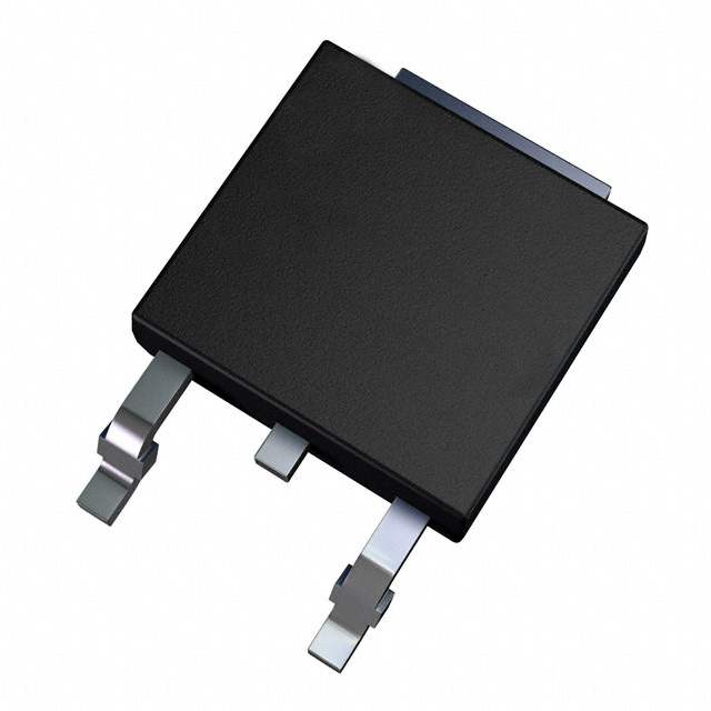
IRLR3915PBF N-Channel MOSFET Equivalent & Substitute Parts
Part Overview
The IRLR3915PBF is an N-Channel MOSFET manufactured by Infineon Technologies, rated for 55V drain-to-source voltage and 30A continuous drain current in a surface mount DPAK package. This device is part of the HEXFET® series and is currently discontinued at DiGi Electronics, necessitating identification of functionally equivalent alternatives for ongoing design support and production requirements.
Substiute Parts
Key Parameters
| Parameter | Value | Unit |
|---|---|---|
| Drain to Source Voltage (Vdss) | 55 | V |
| Continuous Drain Current (Id) @ 25°C | 30 | A (Tc) |
| On-Resistance (Rds On) @ 30A, 10V | 14 | mOhm |
| Gate Threshold Voltage (Vgs(th)) @ 250µA | 3 | V |
| Gate Charge (Qg) @ 10V | 92 | nC |
| Power Dissipation (Max) | 120 | W (Tc) |
| Operating Temperature Range | -55 to 175 | °C (TJ) |
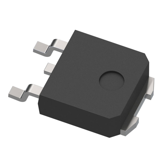
| Package Type | TO-252-3 DPAK | Surface Mount |
| RoHS Status | ROHS3 Compliant |
Substitute Part Grouping Explanation
Substitution eligibility for the IRLR3915PBF is determined by the following critical parameters:
Primary Compatibility Criteria:
- Drain-to-Source Voltage (Vdss): Must equal or exceed 55V
- Continuous Drain Current (Id): Must equal or exceed 30A at 25°C
- Package Type: Must be TO-252-3 DPAK (surface mount, identical pinout)
- FET Type: N-Channel MOSFET technology
- Operating Temperature Range: Must support -55°C to 175°C minimum
Secondary Compatibility Factors:
- On-Resistance (Rds On): Lower values indicate improved performance; values within ±20% of original are functionally compatible
- Gate Charge (Qg): Lower values reduce switching losses; values within ±50% are acceptable
- Power Dissipation: Must support thermal requirements of the application
All four substitute parts meet or exceed the primary compatibility criteria and maintain functional equivalence within the specified electrical and mechanical parameters.
Parameter Comparison
| Parameter | IRLR3915PBF (Main) | IPD35N10S3L26ATMA1 | FDD5353 | STD60NF55LAT4 | STD60NF55LT4 | Unit |
|---|---|---|---|---|---|---|
| Manufacturer | Infineon | Infineon | onsemi | STMicroelectronics | STMicroelectronics | |
| Series | HEXFET® | OptiMOS™ | PowerTrench® | SuperFET® II | STripFET™ II | |
| Product Status | Discontinued | Active | Active | Active | Active | |
| Vdss | 55 | 100 | 60 | 55 | 55 | V |
| Id @ 25°C | 30 | 35 | 50 (Tc) | 60 | 60 | A |
| Rds On @ 10V | 14 | 24 | 12.3 | 15 | 15 | mOhm |
| Vgs(th) @ 250µA | 3 | 2.4 | 3 | 2 | 2 | V |
| Qg @ 10V | 92 | 39 | 65 | 40 | 56 | nC |
| Power Dissipation (Max) | 120 | 71 | 69 (Tc) | 110 | 100 | W |
| Operating Temp Range | -55 to 175 | -55 to 175 | -55 to 150 | -55 to 175 | -55 to 175 | °C |
| Package | TO-252-3 DPAK | TO-252-3 DPAK | TO-252-3 DPAK | TO-252 DPAK | TO-252-3 DPAK | |
| RoHS Status | ROHS3 Compliant | ROHS3 Compliant | ROHS3 Compliant | ROHS3 Compliant | ROHS3 Compliant | |
| Inventory Status | 1151 Pcs | 8550 Pcs | 20200 Pcs | 2900 Pcs | 17810 Pcs |
Engineering Selection Recommendations
STD60NF55LT4 (Primary Recommendation)
The STD60NF55LT4 from STMicroelectronics provides the closest electrical match to the IRLR3915PBF. Both devices share identical Vdss (55V) and equivalent Rds On specifications (15mOhm @ 30A, 10V). The STD60NF55LT4 offers doubled continuous drain current capability (60A vs. 30A), maintaining the same operating temperature range (-55°C to 175°C). This device is in active production status with 17,810 units in stock and carries full ROHS3 compliance and AEC-Q101 automotive qualification.
STD60NF55LAT4 (Secondary Recommendation)
The STD60NF55LAT4 is functionally equivalent to the STD60NF55LT4 with identical electrical specifications and automotive-grade qualification (AEC-Q101). Power dissipation is rated at 110W versus 100W for the LT4 variant. Both STMicroelectronics devices maintain pin-compatible DPAK packaging and support the full operating temperature range.
FDD5353 (Alternative for Current-Constrained Applications)
The FDD5353 from onsemi provides the lowest on-resistance (12.3mOhm @ 10.7A, 10V) among substitute options and supports 50A continuous drain current at Tc. This device is suitable for applications where thermal management and efficiency are prioritized. Operating temperature range extends to 150°C maximum, which is 25°C lower than the original specification. Inventory availability is highest at 20,200 units.
IPD35N10S3L26ATMA1 (Higher Voltage Alternative)
The IPD35N10S3L26ATMA1 from Infineon offers elevated Vdss rating (100V) with 35A continuous drain current. This device is appropriate for applications requiring higher voltage headroom or where circuit redesign permits voltage derating. Gate charge is significantly reduced (39nC vs. 92nC), resulting in lower switching losses. Active production status with 8,550 units available.
Compliance and Certification:
All substitute parts maintain ROHS3 compliance and REACH unaffected status, matching the original device. STMicroelectronics options include AEC-Q101 automotive qualification, suitable for automotive and industrial applications requiring enhanced reliability documentation.
Frequently Asked Questions (FAQ)
Q: Can the IPD35N10S3L26ATMA1 be used as a direct replacement for the IRLR3915PBF?
A: The IPD35N10S3L26ATMA1 is electrically compatible but not a direct replacement. The higher Vdss rating (100V vs. 55V) and different on-resistance characteristics require circuit evaluation. Applications operating below 55V can use this device; however, gate drive characteristics differ due to lower gate charge (39nC vs. 92nC), which may affect switching performance in existing circuits.
Q: What is the primary difference between STD60NF55LT4 and STD60NF55LAT4?
A: Both devices share identical electrical specifications and DPAK packaging. The primary difference is automotive qualification: STD60NF55LAT4 carries AEC-Q101 certification for automotive applications, while STD60NF55LT4 is the industrial-grade variant. Power dissipation ratings differ slightly (110W vs. 100W). Selection depends on application requirements and qualification documentation needs.
Q: Is the FDD5353 suitable for applications requiring the full -55°C to 175°C temperature range?
A: The FDD5353 operating temperature range extends to 150°C maximum, which is 25°C below the IRLR3915PBF specification. Applications requiring operation at temperatures between 150°C and 175°C must use STMicroelectronics or Infineon alternatives (STD60NF55LT4, STD60NF55LAT4, or IPD35N10S3L26ATMA1).
Q: Are all substitute parts available in identical packaging?
A: All substitute parts use TO-252-3 DPAK surface mount packaging with identical pinout (2 leads + tab). Physical dimensions and PCB footprints are compatible. No layout modifications are required for package substitution.
Q: How do gate charge differences affect circuit performance?
A: Gate charge (Qg) determines the energy required to switch the MOSFET. The IRLR3915PBF requires 92nC at 10V, while substitutes range from 39nC (IPD35N10S3L26ATMA1) to 65nC (FDD5353). Lower gate charge reduces switching losses and allows faster switching speeds. Existing gate driver circuits designed for 92nC will function with lower Qg devices but may exhibit improved efficiency and reduced heat generation.
Q: Which substitute offers the best thermal performance?
A: The FDD5353 provides the lowest on-resistance (12.3mOhm), resulting in the lowest conduction losses and superior thermal performance in high-current applications. However, its 150°C maximum operating temperature limits use in high-temperature environments. For applications requiring both low on-resistance and full temperature range support, the STD60NF55LT4 (15mOhm, 175°C max) provides optimal balance.
Q: Can these devices be used interchangeably in existing PCB designs?
A: Yes, all substitute parts are pin-compatible with identical DPAK packaging. PCB designs require no modification. However, circuit performance characteristics such as switching speed and thermal behavior may differ due to variations in gate charge and on-resistance. Thermal analysis should be performed if power dissipation requirements approach device ratings.
Alternative Parts

SJ6012L2TP
Littelfuse Inc.
6 Alternative Parts

JMK107BBJ476MA-RE
Taiyo Yuden
10 Alternative Parts

GMK107BBJ475MA-T
Taiyo Yuden
5 Alternative Parts
SJ6020N2ARP
Littelfuse Inc.
3 Alternative Parts
SJ6025R2ATP
Littelfuse Inc.
4 Alternative Parts

2474-05L
API Delevan Inc.
1 Alternative Parts

4590R-684K
API Delevan Inc.
1 Alternative Parts

CM6560R-334
API Delevan Inc.
1 Alternative Parts

CM6460-104
API Delevan Inc.
1 Alternative Parts

5526-12
API Delevan Inc.
1 Alternative Parts