


Request Quote
(Ships tomorrow)
IRFS450B N-Channel MOSFET 500V 9.6A Equivalent & Substitute Parts
Part Overview
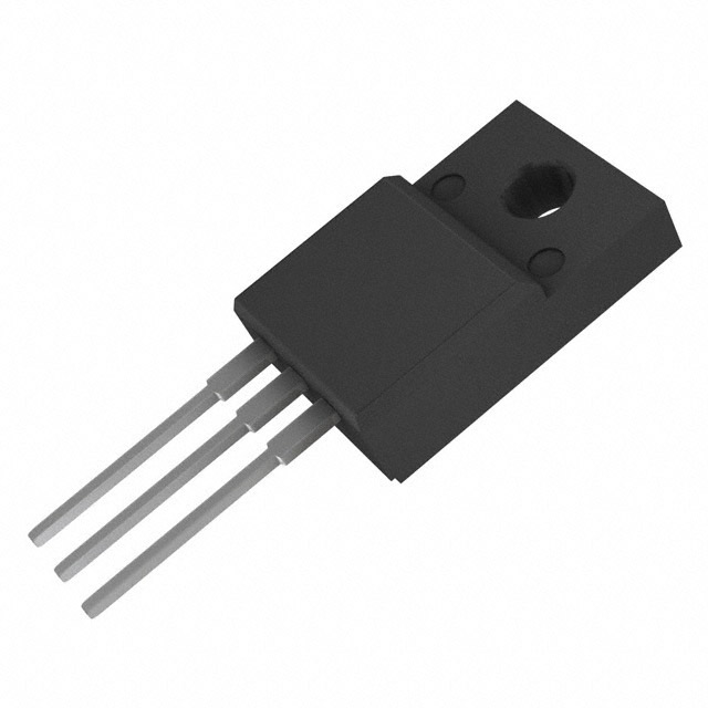
The IRFS450B is an N-Channel MOSFET manufactured by onsemi, rated for 500V drain-to-source voltage with 9.6A continuous drain current at 25°C. This device is packaged in a TO-3PF through-hole configuration and is designed for high-voltage switching applications requiring moderate current handling.
The IRFS450B is classified as obsolete. Locating equivalent or substitute components is necessary to support ongoing maintenance, repair, and redesign activities where this part is specified in existing designs or inventory management requires functional alternatives.
Substiute Parts
Key Parameters
| Parameter | Value | Unit |
|---|---|---|
| Drain-to-Source Voltage (Vdss) | 500 | V |
| Continuous Drain Current (Id) @ 25°C | 9.6 | A (Tc) |
| On-State Resistance (Rds On Max) @ Id, Vgs | 390 mOhm @ 4.8A, 10V | mOhm |
| Gate Threshold Voltage (Vgs(th) Max) @ Id | 4 | V @ 250µA |
| Gate Charge (Qg Max) @ Vgs | 113 | nC @ 10V |
| Power Dissipation (Max) | 96 | W (Tc) |
| Operating Temperature Range | -55 to 150 | °C (TJ) |
| Mounting Type | Through Hole | — |
| Package Type | TO-3PF | — |
Substitute Part Grouping Explanation
Substitution of the IRFS450B is determined by the following critical electrical and mechanical parameters:
Electrical Compatibility Criteria:
- Drain-to-Source Voltage (Vdss) must equal or exceed 500V
- Continuous Drain Current (Id) must meet or exceed 9.6A at 25°C
- Gate Threshold Voltage (Vgs(th)) must be compatible with existing gate drive circuits
- Maximum Gate Voltage (Vgs Max) must be ±30V or greater
- Operating Temperature Range must span -55°C to 150°C or equivalent
Mechanical Compatibility Criteria:
- Mounting Type: Through Hole
- Package compatibility with TO-3P family configurations
The FDA18N50 manufactured by Fairchild Semiconductor meets these substitution criteria. It maintains identical Vdss (500V), exceeds the minimum Id requirement (19A vs. 9.6A), operates across the same temperature range (-55°C to 150°C), and is available in a compatible TO-3P through-hole package (TO-3PN).
Parameter Comparison
| Parameter | IRFS450B (onsemi) | FDA18N50 (Fairchild) | Unit |
|---|---|---|---|
| FET Type | N-Channel | N-Channel | — |
| Technology | MOSFET (Metal Oxide) | MOSFET (Metal Oxide) | — |
| Drain-to-Source Voltage (Vdss) | 500 | 500 | V |
| Continuous Drain Current (Id) @ 25°C | 9.6 | 19 | A (Tc) |
| Drive Voltage (Max Rds On) | 10 | 10 | V |
| Rds On (Max) @ Id, Vgs | 390 mOhm @ 4.8A, 10V | 265 mOhm @ 9.5A, 10V | mOhm |
| Gate Threshold Voltage (Vgs(th) Max) @ Id | 4 | 5 | V @ 250µA |
| Gate Charge (Qg Max) @ Vgs | 113 | 60 | nC @ 10V |
| Vgs (Max) | ±30 | ±30 | V |
| Input Capacitance (Ciss Max) @ Vds | 3800 | 2860 | pF @ 25V |
| Power Dissipation (Max) | 96 | 239 | W (Tc) |
| Operating Temperature Range | -55 to 150 | -55 to 150 | °C (TJ) |
| Mounting Type | Through Hole | Through Hole | — |
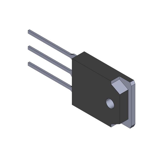
| Package Type | TO-3PF | TO-3PN | — |
| Product Status | Obsolete | Active | — |
Engineering Selection Recommendations
FDA18N50 as Primary Substitute:
The FDA18N50 is the recommended substitute for the IRFS450B based on the following engineering factors:
-
Electrical Equivalence: Both devices share identical Vdss (500V) and operating temperature range (-55°C to 150°C). The FDA18N50 provides higher continuous drain current (19A vs. 9.6A), lower on-state resistance (265 mOhm vs. 390 mOhm), and reduced gate charge (60 nC vs. 113 nC), resulting in improved thermal performance and switching efficiency.
-
Package Compatibility: Both devices use TO-3P family through-hole packages (TO-3PF and TO-3PN). Physical pin configurations are compatible with existing PCB layouts and socket designs.
-
Product Status: The FDA18N50 is classified as Active, ensuring continued availability and supply chain support. The IRFS450B is Obsolete, making the FDA18N50 the appropriate long-term alternative.
-
Compliance: The FDA18N50 carries EAR99 export classification and HTSUS code 8542.39.0001, consistent with regulatory requirements for high-voltage semiconductor components.
-
Gate Drive Compatibility: The FDA18N50 maintains Vgs(th) Max of 5V @ 250µA and Vgs Max of ±30V, ensuring compatibility with existing gate drive circuits designed for the IRFS450B.
Frequently Asked Questions (FAQ)
Q: Can the FDA18N50 directly replace the IRFS450B in existing designs?
A: Yes. Both devices are N-Channel MOSFETs with 500V Vdss, identical operating temperature range, and compatible TO-3P through-hole packages. The FDA18N50 exceeds the IRFS450B in continuous drain current and power dissipation, making it suitable for direct substitution. Pin-to-pin compatibility exists between TO-3PF and TO-3PN packages.
Q: What are the key differences between these two devices?
A: The FDA18N50 provides superior electrical performance: 19A continuous drain current versus 9.6A, lower on-state resistance (265 mOhm vs. 390 mOhm), and reduced gate charge (60 nC vs. 113 nC). Power dissipation capability is significantly higher (239W vs. 96W). These improvements result in lower heat generation and faster switching characteristics.
Q: Are there any gate drive circuit modifications required?
A: No modifications are required. Both devices operate with identical maximum gate voltages (±30V) and similar gate threshold voltages (4V vs. 5V). Existing gate drive circuits designed for the IRFS450B will function with the FDA18N50 without adjustment.
Q: How do the package types differ between IRFS450B and FDA18N50?
A: The IRFS450B uses TO-3PF packaging, while the FDA18N50 uses TO-3PN packaging. Both are TO-3P family through-hole packages with compatible pin configurations and mechanical dimensions suitable for standard PCB layouts and socket installations.
Q: Why is the IRFS450B classified as obsolete?
A: The IRFS450B is no longer in active production by onsemi. The FDA18N50 represents the current-generation equivalent from Fairchild Semiconductor, offering improved performance characteristics and guaranteed long-term availability.
Q: What is the impact of lower gate charge in the FDA18N50?
A: Lower gate charge (60 nC vs. 113 nC) reduces the energy required to switch the device on and off, resulting in lower gate drive power consumption and faster switching transitions. This improves overall circuit efficiency and thermal performance.
Q: Are thermal management considerations different between these devices?
A: The FDA18N50 has significantly higher power dissipation capability (239W vs. 96W) and lower on-state resistance, resulting in reduced heat generation at equivalent current levels. Existing thermal management solutions designed for the IRFS450B will provide adequate cooling for the FDA18N50 in most applications.
Alternative Parts

SJ6012L2TP
Littelfuse Inc.
6 Alternative Parts

JMK107BBJ476MA-RE
Taiyo Yuden
10 Alternative Parts

GMK107BBJ475MA-T
Taiyo Yuden
5 Alternative Parts
SJ6020N2ARP
Littelfuse Inc.
3 Alternative Parts
SJ6025R2ATP
Littelfuse Inc.
4 Alternative Parts

2474-05L
API Delevan Inc.
1 Alternative Parts

4590R-684K
API Delevan Inc.
1 Alternative Parts

CM6560R-334
API Delevan Inc.
1 Alternative Parts

CM6460-104
API Delevan Inc.
1 Alternative Parts

5526-12
API Delevan Inc.
1 Alternative Parts