


Request Quote
(Ships tomorrow)
IRFS23N15D N-Channel MOSFET 150V 23A Equivalent & Substitute Parts
Part Overview
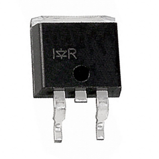
The IRFS23N15D is an N-Channel MOSFET manufactured by Infineon Technologies, designed for surface mount applications in the D2PAK package. This device operates at 150V drain-to-source voltage with a continuous drain current rating of 23A at 25°C case temperature. The part is classified as obsolete, making identification of suitable substitute components necessary for ongoing design support and procurement continuity.
Substiute Parts
Key Parameters
| Parameter | Value | Unit |
|---|---|---|
| Drain to Source Voltage (Vdss) | 150 | V |
| Continuous Drain Current (Id) @ 25°C | 23 | A (Tc) |
| On-State Resistance (Rds On) @ 14A, 10V | 90 | mOhm |
| Gate Threshold Voltage (Vgs(th)) @ 250µA | 5.5 | V |
| Gate Charge (Qg) @ 10V | 56 | nC |
| Maximum Gate Voltage (Vgs) | ±30 | V |
| Input Capacitance (Ciss) @ 25V | 1200 | pF |
| Power Dissipation (Max) | 3.8 (Ta), 136 (Tc) | W |
| Operating Temperature Range | -55 to 175 | °C (TJ) |
| Package Type | TO-263-3, D2PAK | - |
| Mounting Type | Surface Mount | - |
Substitute Part Grouping Explanation
Substitution of the IRFS23N15D is determined by strict alignment of the following electrical and mechanical parameters:
Critical Matching Parameters:
- Drain-to-Source Voltage (Vdss): Must equal or exceed 150V
- Package Type: Must be TO-263-3 or D2PAK (2 Leads + Tab) for mechanical and thermal compatibility
- Mounting Type: Must be Surface Mount
- FET Type: Must be N-Channel MOSFET (Metal Oxide technology)
- Operating Temperature Range: Must support -55°C to 175°C
Performance Parameters for Functional Equivalence:
- Continuous Drain Current (Id): Substitute must meet or exceed 23A at case temperature
- On-State Resistance (Rds On): Lower or equal values indicate improved performance
- Gate Threshold Voltage (Vgs(th)): Must be within acceptable drive circuit compatibility range
- Gate Charge (Qg): Affects switching speed and drive requirements
- Maximum Gate Voltage (Vgs): Must accommodate circuit drive voltage levels
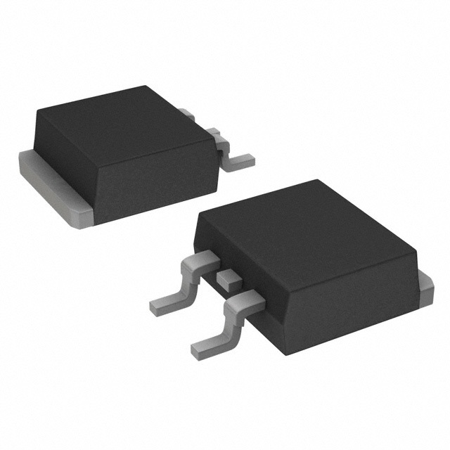
The AOB256L from Alpha & Omega Semiconductor Inc. meets all critical matching parameters and is classified as an active product, providing long-term availability and support.
Parameter Comparison
| Parameter | IRFS23N15D (Infineon) | AOB256L (Alpha & Omega) | Unit |
|---|---|---|---|
| Drain to Source Voltage (Vdss) | 150 | 150 | V |
| Continuous Drain Current (Id) @ 25°C | 23 (Tc) | 19 (Tc) | A |
| On-State Resistance (Rds On) | 90 @ 14A, 10V | 85 @ 10A, 10V | mOhm |
| Gate Threshold Voltage (Vgs(th)) @ 250µA | 5.5 | 2.8 | V |
| Gate Charge (Qg) @ 10V | 56 | 22 | nC |
| Maximum Gate Voltage (Vgs) | ±30 | ±20 | V |
| Input Capacitance (Ciss) | 1200 @ 25V | 1165 @ 75V | pF |
| Power Dissipation (Max) | 3.8 (Ta), 136 (Tc) | 2.1 (Ta), 83 (Tc) | W |
| Operating Temperature Range | -55 to 175 | -55 to 175 | °C (TJ) |
| Package Type | TO-263-3, D2PAK | TO-263-3, D2PAK | - |
| Mounting Type | Surface Mount | Surface Mount | - |
| Product Status | Obsolete | Active | - |
| RoHS Status | RoHS non-compliant | ROHS3 Compliant | - |
Engineering Selection Recommendations
Product Status Consideration: The IRFS23N15D is classified as obsolete. The AOB256L is an active product with confirmed inventory availability (10,265 pieces in stock), ensuring procurement continuity and long-term supply chain stability.
Compliance and Certification: The AOB256L is ROHS3 compliant, whereas the IRFS23N15D is RoHS non-compliant. Both devices are REACH unaffected and classified under ECCN EAR99. Selection of the AOB256L aligns with modern regulatory requirements for new designs and manufacturing operations.
Electrical Performance: The AOB256L demonstrates lower gate charge (22 nC versus 56 nC) and lower gate threshold voltage (2.8V versus 5.5V), resulting in faster switching characteristics and reduced drive circuit complexity. The on-state resistance is comparable (85 mOhm versus 90 mOhm), indicating equivalent conduction losses under similar operating conditions.
Current Rating Differential: The AOB256L continuous drain current rating is 19A at case temperature, compared to 23A for the IRFS23N15D. Applications requiring the full 23A rating must evaluate whether the 19A rating of the substitute is sufficient for the intended circuit. Thermal management and duty cycle analysis are necessary for applications operating near maximum current specifications.
Gate Voltage Compatibility: The AOB256L maximum gate voltage is ±20V, compared to ±30V for the IRFS23N15D. Circuits applying gate voltages exceeding ±20V require design modification or alternative component selection.
Frequently Asked Questions (FAQ)
Q: Can the AOB256L directly replace the IRFS23N15D in existing designs?
A: The AOB256L is mechanically and electrically compatible for most applications due to identical package type (TO-263-3, D2PAK) and matching drain-to-source voltage (150V). However, three factors require verification: (1) the continuous drain current requirement must not exceed 19A at case temperature; (2) gate drive circuits must not exceed ±20V; (3) the lower gate threshold voltage (2.8V versus 5.5V) may affect gate drive timing and must be evaluated in the specific circuit context.
Q: What is the significance of the lower gate charge in the AOB256L?
A: Gate charge (Qg) of 22 nC in the AOB256L versus 56 nC in the IRFS23N15D indicates faster switching transitions. This reduces switching losses and allows higher switching frequencies. Gate drive circuits designed for the IRFS23N15D will operate with improved performance margins when driving the AOB256L, provided gate voltage limits (±20V maximum) are observed.
Q: Are there thermal performance differences between these devices?
A: The AOB256L has lower maximum power dissipation ratings (2.1W at ambient temperature, 83W at case temperature) compared to the IRFS23N15D (3.8W at ambient, 136W at case temperature). This reflects the lower continuous drain current rating (19A versus 23A). Thermal design calculations must account for the specific current levels in the application. The on-state resistance values are comparable, so conduction losses per ampere are similar.
Q: Why is RoHS compliance important for this substitution?
A: The AOB256L is ROHS3 compliant while the IRFS23N15D is RoHS non-compliant. New product designs and manufacturing operations in regions with RoHS regulations must use compliant components. The AOB256L meets these regulatory requirements, making it suitable for applications subject to RoHS directives.
Q: What packaging considerations apply to this substitution?
A: Both devices use the TO-263-3 (D2PAK) surface mount package with identical pinout and thermal tab configuration. PCB layouts, solder reflow profiles, and thermal management approaches designed for the IRFS23N15D are directly applicable to the AOB256L without modification. Tape & Reel packaging is available for the AOB256L, supporting automated assembly processes.
Q: How does the gate threshold voltage difference affect circuit operation?
A: The AOB256L gate threshold voltage is 2.8V compared to 5.5V for the IRFS23N15D. This means the AOB256L begins conducting at a lower gate voltage. Gate drive circuits must be evaluated to ensure proper on/off switching behavior. In circuits with marginal gate drive voltage, the lower threshold of the AOB256L may provide improved noise margin. Conversely, circuits relying on the higher threshold of the IRFS23N15D for specific timing characteristics require redesign.
Alternative Parts

SJ6012L2TP
Littelfuse Inc.
6 Alternative Parts

JMK107BBJ476MA-RE
Taiyo Yuden
10 Alternative Parts

GMK107BBJ475MA-T
Taiyo Yuden
5 Alternative Parts
SJ6020N2ARP
Littelfuse Inc.
3 Alternative Parts
SJ6025R2ATP
Littelfuse Inc.
4 Alternative Parts

2474-05L
API Delevan Inc.
1 Alternative Parts

4590R-684K
API Delevan Inc.
1 Alternative Parts

CM6560R-334
API Delevan Inc.
1 Alternative Parts

CM6460-104
API Delevan Inc.
1 Alternative Parts

5526-12
API Delevan Inc.
1 Alternative Parts