


Request Quote
(Ships tomorrow)
IRF5852 Equivalent & Substitute Parts
Part Overview
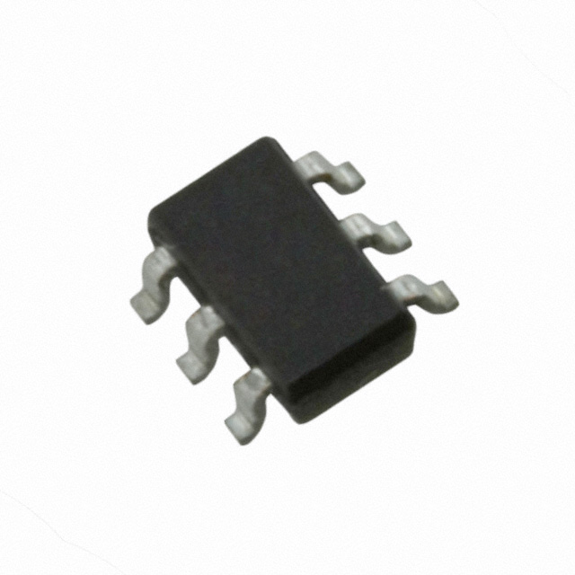
The IRF5852 is a dual N-channel MOSFET array manufactured by Infineon Technologies, designed for surface mount applications in logic-level gate switching circuits. This device features a 20V drain-to-source voltage rating with 2.7A continuous drain current capability and is housed in a 6-TSOP package configuration.
The IRF5852 is classified as an obsolete product. Identifying suitable substitute components is necessary to maintain design continuity, ensure component availability, and support ongoing production requirements for applications currently utilizing this device.
Substiute Parts
Key Parameters
| Parameter | Value | Specification |
|---|---|---|
| Drain to Source Voltage (Vdss) | 20V | Maximum rated voltage |
| Continuous Drain Current (Id) @ 25°C | 2.7A | Maximum continuous current |
| On-State Resistance (Rds On) @ Id, Vgs | 90mOhm @ 2.7A, 4.5V | Maximum drain-source on-state resistance |
| Gate Threshold Voltage (Vgs(th)) @ Id | 1.25V @ 250µA | Maximum gate threshold voltage |
| Gate Charge (Qg) @ Vgs | 6nC @ 4.5V | Maximum gate charge |
| Input Capacitance (Ciss) @ Vds | 400pF @ 15V | Maximum input capacitance |
| Power Dissipation (Max) | 960mW | Maximum power rating |
| Configuration | 2 N-Channel (Dual) | Device architecture |
| Package Type | SOT-23-6 Thin / TSOP-6 | Surface mount package |
| Technology | MOSFET (Metal Oxide) | Semiconductor technology |
| FET Feature | Logic Level Gate | Gate drive characteristic |
Substitute Part Grouping Explanation
Substitute components for the IRF5852 are identified based on strict electrical and mechanical parameter matching within the dual N-channel MOSFET category. The substitution criteria are:
Critical Matching Parameters:
- Drain-to-Source Voltage (Vdss): 20V
- Continuous Drain Current (Id): 2.7A minimum
- Package Configuration: Dual N-Channel
- Mounting Type: Surface Mount
- Package Style: SOT-23-6 / TSOP-6 compatible footprint
Acceptable Parameter Ranges for Substitution:
- On-State Resistance (Rds On): Equal to or lower than 90mOhm @ 2.7A, 4.5V
- Gate Threshold Voltage (Vgs(th)): Within 1.25V @ 250µA specification
- Gate Charge (Qg): Equal to or lower than 6nC @ 4.5V
- Input Capacitance (Ciss): Equal to or lower than 400pF @ 15V
- Power Dissipation: Equal to or greater than 960mW
The FDC6305N from onsemi meets all critical matching parameters and demonstrates improved electrical characteristics in key performance metrics.
Parameter Comparison
| Parameter | IRF5852 (Infineon) | FDC6305N (onsemi) | Compatibility |
|---|---|---|---|
| Drain to Source Voltage (Vdss) | 20V | 20V | Match |
| Continuous Drain Current (Id) @ 25°C | 2.7A | 2.7A | Match |
| Rds On (Max) @ Id, Vgs | 90mOhm @ 2.7A, 4.5V | 80mOhm @ 2.7A, 4.5V | Improved |
| Vgs(th) (Max) @ Id | 1.25V @ 250µA | 1.5V @ 250µA | Within tolerance |
| Gate Charge (Qg) (Max) @ Vgs | 6nC @ 4.5V | 5nC @ 4.5V | Improved |
| Input Capacitance (Ciss) (Max) @ Vds | 400pF @ 15V | 310pF @ 10V | Improved |
| Power - Max | 960mW | 700mW | Lower rating |
| Configuration | 2 N-Channel (Dual) | 2 N-Channel (Dual) | Match |
| Package / Case | SOT-23-6 Thin, TSOP-23-6 | SOT-23-6 Thin, TSOP-23-6 | Match |
| Mounting Type | Surface Mount | Surface Mount | Match |
| Technology | MOSFET (Metal Oxide) | MOSFET (Metal Oxide) | Match |
| Product Status | Obsolete | Active | Availability advantage |
| RoHS Status | RoHS non-compliant | ROHS3 Compliant | Compliance advantage |
Engineering Selection Recommendations
FDC6305N as Primary Substitute:
The FDC6305N from onsemi is the qualified substitute for the IRF5852. This substitution is supported by the following engineering factors:
Electrical Compatibility: All critical electrical parameters match or exceed IRF5852 specifications. The FDC6305N demonstrates superior performance in on-state resistance (80mOhm vs. 90mOhm), gate charge (5nC vs. 6nC), and input capacitance (310pF vs. 400pF). These improvements result in lower switching losses and reduced gate drive requirements.
Package and Mechanical Compatibility: Both devices utilize identical SOT-23-6 / TSOP-6 surface mount packaging, ensuring direct PCB footprint compatibility without layout modifications.
Product Status and Availability: The IRF5852 is classified as obsolete, while the FDC6305N maintains active production status with substantial inventory availability (105,100 pieces in stock versus 917 pieces for the IRF5852). This availability differential supports long-term supply chain continuity.
Regulatory Compliance: The FDC6305N is ROHS3 compliant, whereas the IRF5852 is RoHS non-compliant. This compliance advantage aligns with current regulatory requirements for electronic component procurement.
Application Suitability: The FDC6305N is suitable for direct substitution in applications where the IRF5852 was previously specified, provided that the lower maximum power dissipation rating (700mW vs. 960mW) does not exceed application thermal requirements. Thermal analysis of the specific application circuit is required to confirm adequate power dissipation margin.
Frequently Asked Questions (FAQ)
Q: Can the FDC6305N be used as a direct replacement for the IRF5852 without circuit modifications?
A: The FDC6305N is electrically and mechanically compatible with the IRF5852 for direct PCB substitution. However, thermal design verification is required. The FDC6305N has a lower maximum power dissipation rating (700mW vs. 960mW). If the application circuit dissipates power near or exceeding 700mW in the MOSFET, thermal analysis must confirm adequate margin. The improved on-state resistance of the FDC6305N (80mOhm vs. 90mOhm) typically results in lower power dissipation, which may offset the lower power rating.
Q: Are there any gate drive differences between the IRF5852 and FDC6305N?
A: Both devices feature logic-level gate operation. The gate threshold voltage of the FDC6305N (1.5V @ 250µA) is slightly higher than the IRF5852 (1.25V @ 250µA), but both operate within standard logic-level gate specifications. Gate drive circuits designed for the IRF5852 will function with the FDC6305N without modification. The lower gate charge of the FDC6305N (5nC vs. 6nC) may result in slightly faster switching transitions.
Q: What is the significance of the improved on-state resistance in the FDC6305N?
A: The FDC6305N exhibits lower on-state resistance (80mOhm vs. 90mOhm) at identical operating conditions. This 11% reduction in Rds On decreases conduction losses in the MOSFET, resulting in lower power dissipation and reduced thermal generation. This improvement is particularly beneficial in high-frequency switching applications or designs operating near thermal limits.
Q: Is the FDC6305N package footprint identical to the IRF5852?
A: Yes. Both devices are housed in SOT-23-6 / TSOP-6 surface mount packages with identical pin configurations and PCB footprints. No layout modifications are required for substitution.
Q: What is the impact of the lower input capacitance in the FDC6305N?
A: The FDC6305N has lower input capacitance (310pF @ 10V vs. 400pF @ 15V). Lower input capacitance reduces gate charge requirements and enables faster switching transitions with lower gate drive power consumption. This characteristic is advantageous in high-frequency applications and reduces electromagnetic interference (EMI) generation.
Q: Are there compliance or regulatory differences between these devices?
A: The FDC6305N is ROHS3 compliant, while the IRF5852 is RoHS non-compliant. For applications subject to RoHS regulations or customer requirements, the FDC6305N is the appropriate choice. Both devices are REACH unaffected and classified under ECCN EAR99.
Q: What inventory considerations should be evaluated?
A: The IRF5852 has limited inventory (917 pieces) and obsolete product status, indicating declining availability. The FDC6305N has substantial inventory (105,100 pieces) and active production status, supporting long-term supply chain reliability and cost stability.
Alternative Parts

SJ6012L2TP
Littelfuse Inc.
6 Alternative Parts

JMK107BBJ476MA-RE
Taiyo Yuden
10 Alternative Parts

GMK107BBJ475MA-T
Taiyo Yuden
5 Alternative Parts
SJ6020N2ARP
Littelfuse Inc.
3 Alternative Parts
SJ6025R2ATP
Littelfuse Inc.
4 Alternative Parts

2474-05L
API Delevan Inc.
1 Alternative Parts

4590R-684K
API Delevan Inc.
1 Alternative Parts

CM6560R-334
API Delevan Inc.
1 Alternative Parts

CM6460-104
API Delevan Inc.
1 Alternative Parts

5526-12
API Delevan Inc.
1 Alternative Parts