


Request Quote
(Ships tomorrow)
IPW65R190CFDFKSA1 Equivalent & Substitute Parts
Part Overview
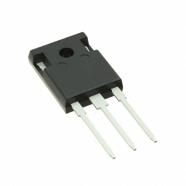
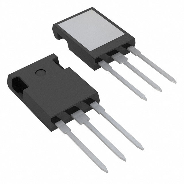
The IPW65R190CFDFKSA1 is an N-Channel 650V 17.5A MOSFET manufactured by Infineon Technologies in the CoolMOS™ series, housed in a TO-247-3 through-hole package. This device is rated for 151W power dissipation and features a maximum on-state resistance of 190mOhm at specified conditions. The part is currently discontinued at DiGi Electronics, necessitating identification of functionally equivalent alternatives for ongoing system support and new designs. Substitute parts must maintain electrical compatibility across voltage, current, and thermal specifications while accommodating packaging and availability constraints.
Substiute Parts
Key Parameters
| Parameter | Value | Unit | Condition |
|---|---|---|---|
| Drain to Source Voltage (Vdss) | 650 | V | Maximum rating |
| Continuous Drain Current (Id) @ 25°C | 17.5 | A | Tc |
| On-State Resistance (Rds On Max) | 190 | mOhm | @ 7.3A, 10V Vgs |
| Gate Charge (Qg Max) | 68 | nC | @ 10V Vgs |
| Power Dissipation (Max) | 151 | W | Tc |
| Operating Temperature Range | -55 to 150 | °C | TJ |
| Package Type | TO-247-3 | — | Through hole |
| Gate Threshold Voltage (Vgs th Max) | 4.5 | V | @ 730µA Id |
| Input Capacitance (Ciss Max) | 1850 | pF | @ 100V Vds |
Substitute Part Grouping Explanation
Substitution eligibility for the IPW65R190CFDFKSA1 is determined by the following critical parameters:
Primary Compatibility Criteria:
- Drain to Source Voltage (Vdss) must equal or exceed 650V
- Continuous Drain Current (Id) must meet or exceed 17.5A at 25°C
- On-State Resistance (Rds On) must not exceed 190mOhm at rated conditions
- Package must be TO-247-3 or compatible through-hole variant
- Operating temperature range must encompass -55°C to 150°C
Secondary Compatibility Factors:
- Gate Charge (Qg) and Input Capacitance (Ciss) affect switching performance and circuit design
- Power Dissipation rating must support thermal requirements of the application
- Gate Threshold Voltage (Vgs th) and maximum gate voltage (±20V) ensure gate drive compatibility
Substitutes are grouped into two categories: Direct Equivalents (matching all primary criteria with identical or superior ratings) and Functional Alternatives (meeting primary criteria with trade-offs in secondary parameters).
Parameter Comparison
| Parameter | IPW65R190CFDFKSA1 | IPW65R190CFDFKSA2 | IPW65R155CFD7XKSA1 | FCH190N65F-F155 | IXFR48N60Q3 | IXFX44N80P |
|---|---|---|---|---|---|---|
| Manufacturer | Infineon | Infineon | Infineon | onsemi | IXYS | IXYS |
| Vdss (V) | 650 | 650 | 650 | 650 | 600 | 800 |
| Id @ 25°C (A) | 17.5 | 17.5 | 15 | 20.6 | 32 | 44 |
| Rds On Max (mOhm) | 190 | 190 | 155 | 190 | 154 | 190 |
| Qg Max (nC) | 68 | 68 | 28 | 78 | 140 | 198 |
| Power Dissipation Max (W) | 151 | 151 | 77 | 208 | 500 | 1040 |
| Ciss Max (pF) | 1850 | 1850 | 1283 | 3225 | 7020 | 12000 |
| Operating Temp Range (°C) | -55 to 150 | -55 to 150 | -55 to 150 | -55 to 150 | -55 to 150 | -55 to 150 |
| Package | TO-247-3 | TO-247-3 | TO-247-3 | TO-247-3 | ISOPLUS247™ | PLUS247™-3 |
| Product Status | Discontinued | Active | Active | Not For New Designs | Active | Active |
| RoHS Status | ROHS3 Compliant | ROHS3 Compliant | ROHS3 Compliant | ROHS3 Compliant | ROHS3 Compliant | ROHS3 Compliant |
Engineering Selection Recommendations
Direct Equivalent (Recommended for Replacement):
IPW65R190CFDFKSA2 is the primary substitute for the discontinued IPW65R190CFDFKSA1. Both devices share identical electrical specifications: 650V Vdss, 17.5A continuous drain current, 190mOhm on-state resistance, and 151W power dissipation. The IPW65R190CFDFKSA2 is currently active in production with ROHS3 compliance and unlimited moisture sensitivity level. The only difference is packaging configuration (Tube vs. original), which does not affect electrical performance. This part provides direct pin-compatible replacement with no circuit redesign required.
Functional Alternative (Lower Current Rating):
IPW65R155CFD7XKSA1 is suitable for applications where continuous drain current can be reduced to 15A. This CoolMOS™ CFD7 device maintains 650V Vdss and improves on-state resistance to 155mOhm, reducing conduction losses. Gate charge is significantly lower at 28nC versus 68nC, improving switching efficiency. Power dissipation is reduced to 77W. This part is active and ROHS3 compliant. Selection requires verification that 15A current rating meets application requirements.
Functional Alternative (Higher Current Rating):
FCH190N65F-F155 (onsemi) provides 20.6A continuous drain current at 650V with matching 190mOhm on-state resistance. Power dissipation increases to 208W. Gate charge is 78nC. This part is marked "Not For New Designs" and should be used only for legacy system support. ROHS3 compliant.
Functional Alternative (Lower Voltage Rating):
IXFR48N60Q3 (IXYS) operates at 600V Vdss with significantly higher current capability (32A) and lower on-state resistance (154mOhm). Power dissipation reaches 500W. Gate charge is 140nC. Package is ISOPLUS247™, compatible with TO-247-3 footprints. This part is active and ROHS3 compliant. Selection requires confirmation that 600V rating is acceptable for the application.
Functional Alternative (Higher Voltage Rating):
IXFX44N80P (IXYS) operates at 800V Vdss with 44A continuous current and 190mOhm on-state resistance. Power dissipation is 1040W. Gate charge is 198nC. Package is PLUS247™-3 variant. This part is active and ROHS3 compliant. Selection is appropriate for applications requiring higher voltage margin or higher current capability.
Frequently Asked Questions (FAQ)
Q: Can IPW65R190CFDFKSA2 be used as a direct replacement for IPW65R190CFDFKSA1?
A: Yes. Both parts are electrically identical with 650V Vdss, 17.5A continuous drain current, 190mOhm on-state resistance, and 151W power dissipation. The IPW65R190CFDFKSA2 is the active production equivalent and requires no circuit modifications.
Q: What is the difference between the original part and IPW65R190CFDFKSA2?
A: The primary difference is packaging configuration. The original uses standard PG-TO247-3-1 packaging, while the IPW65R190CFDFKSA2 uses PG-TO247-3-41 (Tube packaging). Electrical specifications and pin configuration are identical. Both use TO-247-3 through-hole package format.
Q: Can I use IPW65R155CFD7XKSA1 if my application only requires 15A?
A: Yes, provided your circuit design confirms that 15A continuous drain current is sufficient. This part offers advantages including lower on-state resistance (155mOhm vs. 190mOhm), significantly lower gate charge (28nC vs. 68nC), and reduced power dissipation (77W vs. 151W). These characteristics improve switching efficiency and reduce thermal load.
Q: What are the implications of using IXFR48N60Q3 with its 600V rating instead of 650V?
A: The 600V rating reduces voltage margin by 50V. This substitution is acceptable only if your application's maximum operating voltage does not exceed 600V and includes adequate design margin. The IXFR48N60Q3 offers higher current capability (32A vs. 17.5A) and lower on-state resistance (154mOhm vs. 190mOhm), reducing conduction losses.
Q: Why does IXFX44N80P have such high gate charge (198nC)?
A: The IXFX44N80P is rated for 44A continuous current and 800V Vdss, requiring larger die geometry. Higher gate charge reflects the increased capacitance associated with larger semiconductor structures. This impacts gate drive circuit design and switching frequency capability.
Q: Are all substitute parts RoHS3 compliant?
A: Yes. All listed substitute parts carry ROHS3 Compliant certification, meeting environmental and hazardous substance restrictions for electronic components.
Q: Can ISOPLUS247™ and PLUS247™-3 packages be used in TO-247-3 footprints?
A: ISOPLUS247™ and PLUS247™-3 are mechanical and electrical variants of the TO-247-3 package family. Pin configuration and footprint compatibility must be verified against your PCB design. Consult device datasheets for precise dimensional specifications before PCB layout finalization.
Q: What is the significance of "Not For New Designs" status for FCH190N65F-F155?
A: This designation indicates the part is available for legacy system support and maintenance but should not be selected for new product development. Infineon and onsemi recommend using active-status alternatives for new designs to ensure long-term supply availability and access to latest technology improvements.
Q: How do I determine which substitute is best for my application?
A: Evaluate based on: (1) Required continuous drain current—select parts rated at or above your specification; (2) Maximum operating voltage—ensure Vdss rating exceeds your circuit voltage; (3) Thermal requirements—verify power dissipation rating supports your thermal design; (4) Switching frequency—lower gate charge (Qg) supports higher switching frequencies; (5) Availability and product status—prefer active parts for new designs.
Alternative Parts

SJ6012L2TP
Littelfuse Inc.
6 Alternative Parts

JMK107BBJ476MA-RE
Taiyo Yuden
10 Alternative Parts

GMK107BBJ475MA-T
Taiyo Yuden
5 Alternative Parts
SJ6020N2ARP
Littelfuse Inc.
3 Alternative Parts
SJ6025R2ATP
Littelfuse Inc.
4 Alternative Parts

2474-05L
API Delevan Inc.
1 Alternative Parts

4590R-684K
API Delevan Inc.
1 Alternative Parts

CM6560R-334
API Delevan Inc.
1 Alternative Parts

CM6460-104
API Delevan Inc.
1 Alternative Parts

5526-12
API Delevan Inc.
1 Alternative Parts