


Request Quote
(Ships tomorrow)
IPB65R310CFDATMA1 N-Channel 650V MOSFET Equivalent & Substitute Parts
Part Overview
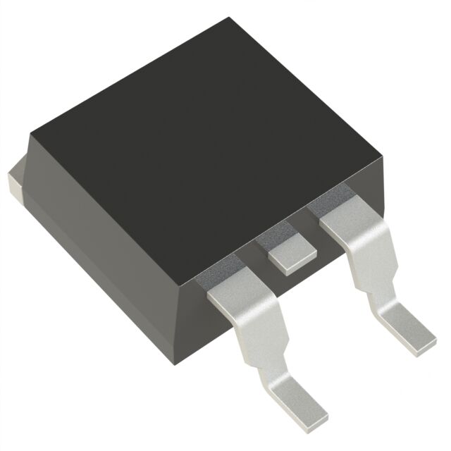
The IPB65R310CFDATMA1 is an N-Channel 650V 11.4A surface mount MOSFET manufactured by Infineon Technologies in the CoolMOS™ series. This device is rated for 104.2W power dissipation and operates across -55°C to 150°C junction temperature range. The part is classified as Obsolete, making equivalent and substitute parts necessary for ongoing design support and procurement continuity. The device is packaged in TO-263-3 (D2PAK) configuration with RoHS3 compliance and unlimited moisture sensitivity rating.
Substiute Parts
Key Parameters
| Parameter | Value | Unit |
|---|---|---|
| Drain to Source Voltage (Vdss) | 650 | V |
| Continuous Drain Current (Id) @ 25°C | 11.4 | A |
| On-State Resistance (Rds On) @ 4.4A, 10V | 310 | mOhm |
| Gate Threshold Voltage (Vgs(th)) @ 400µA | 4.5 | V |
| Gate Charge (Qg) @ 10V | 41 | nC |
| Input Capacitance (Ciss) @ 100V | 1100 | pF |
| Power Dissipation (Max) | 104.2 | W |
| Operating Temperature Range | -55 to 150 | °C |
| Package Type | TO-263-3 (D2PAK) | — |
| Mounting Type | Surface Mount | — |
Substitute Part Grouping Explanation
Substitution eligibility for the IPB65R310CFDATMA1 is determined by the following critical parameters:
Primary Substitution Criteria:
- Drain to Source Voltage (Vdss): 650V or higher
- Continuous Drain Current (Id): 11.4A or higher
- On-State Resistance (Rds On): 310mOhm or lower at specified gate voltage
- Package Type: TO-263-3 (D2PAK) or compatible surface mount package
- Gate Drive Voltage: 10V nominal
- Operating Temperature: -55°C to 150°C minimum
Substitution Categories:
Category 1: Parametric Equivalent (Direct Replacement) IPB65R310CFDATMA2 meets all electrical specifications identically to the main part. This is a direct parametric equivalent with identical Vdss, Id, Rds On, and gate charge characteristics. The primary difference is product status (Active vs. Obsolete) and packaging format (Tape & Reel vs. Cut Tape).
Category 2: Functional Equivalent with Enhanced Performance IXFA12N65X2, SIHB12N60ET1-GE3, and STB18NM80 provide functional equivalence with variations in secondary parameters. These parts maintain the critical voltage and current ratings while offering different Rds On values, gate charge characteristics, and power dissipation ratings. Voltage ratings range from 600V to 800V, accommodating the 650V requirement.
Category 3: Functional Equivalent with Reduced Voltage Rating R6011ENJTL and STB13NM60N operate at 600V Vdss, which is 50V below the main part specification. These parts are suitable only for applications where the 650V rating is not a hard requirement and 600V provides adequate margin.
Category 4: Functional Equivalent with Enhanced Current Rating STB18NM80 provides 17A continuous drain current against the 11.4A requirement, offering additional current headroom while maintaining compatible package and drive voltage specifications.
Parameter Comparison
| Parameter | IPB65R310CFDATMA1 | IPB65R310CFDATMA2 | IXFA12N65X2 | R6011ENJTL | SIHB12N60ET1-GE3 | STB13NM60N | STB18NM80 | STB18NM60DM2 |
|---|---|---|---|---|---|---|---|---|
| Manufacturer | Infineon | Infineon | IXYS | Rohm | Vishay | STMicroelectronics | STMicroelectronics | STMicroelectronics |
| Vdss (V) | 650 | 650 | 650 | 600 | 600 | 600 | 800 | 600 |
| Id @ 25°C (A) | 11.4 | 11.4 | 12 | 11 | 12 | 11 | 17 | 12 |
| Rds On @ 10V (mOhm) | 310 @ 4.4A | 310 @ 4.4A | 310 @ 6A | 390 @ 3.8A | 380 @ 6A | 360 @ 5.5A | 295 @ 8.5A | 295 @ 6A |
| Vgs(th) (V) | 4.5 @ 400µA | 4.5 @ 400µA | 5 @ 250µA | 4 @ 1mA | 4 @ 250µA | 4 @ 250µA | 5 @ 250µA | 5 @ 250µA |
| Qg @ 10V (nC) | 41 | 41 | 18.5 | 32 | 58 | 30 | 70 | 20 |
| Ciss @ Vds (pF) | 1100 @ 100V | 1100 @ 100V | 1134 @ 25V | 670 @ 25V | 937 @ 100V | 790 @ 50V | 2070 @ 50V | 800 @ 100V |
| Power Dissipation (W) | 104.2 | 104.2 | 180 | 40 | 147 | 90 | 190 | 90 |
| Tj Range (°C) | -55 to 150 | -55 to 150 | -55 to 150 | to 150 | -55 to 150 | to 150 | to 150 | to 150 |
| Package | TO-263-3 | TO-263-3 | TO-263AA | LPTS | TO-263 | D2PAK | TO-263 | TO-263 |
| Product Status | Obsolete | Active | Active | Active | Active | Active | Active | Active |
| RoHS3 Compliant | Yes | Yes | Yes | Yes | Not specified | Yes | Yes | Yes |
Engineering Selection Recommendations
Direct Replacement (No Design Changes Required):
IPB65R310CFDATMA2 is the recommended direct replacement for the obsolete IPB65R310CFDATMA1. Both parts are manufactured by Infineon Technologies and share identical electrical specifications: 650V Vdss, 11.4A continuous drain current, 310mOhm Rds On, and 41nC gate charge. The IPB65R310CFDATMA2 is currently Active in product status with 1897 pieces in stock. Both parts are RoHS3 compliant with unlimited moisture sensitivity rating. The only substantive difference is packaging format: the original uses Cut Tape (CT) & Digi-Reel®, while the substitute uses Tape & Reel (TR). This substitution requires no circuit modifications or thermal design changes.
Functional Equivalents with Acceptable Parameter Variations:
IXFA12N65X2 (IXYS) maintains the 650V Vdss requirement with 12A continuous drain current (0.6A higher than the main part). On-state resistance is identical at 310mOhm. Gate charge is significantly lower at 18.5nC, reducing switching losses. Power dissipation rating is higher at 180W. This part is suitable for applications where the additional current capacity and lower gate charge provide design benefits. Package is TO-263AA (IXFA), which is mechanically compatible with TO-263-3 footprints.
STB18NM80 (STMicroelectronics) provides the highest current rating at 17A with 800V Vdss, exceeding both voltage and current requirements. On-state resistance is 295mOhm at 8.5A, slightly better than the main part. Gate charge is 70nC, higher than the main part, resulting in increased switching losses. Power dissipation is 190W. This part is suitable for applications requiring higher voltage margin or current headroom. Package is TO-263 (D2PAK), directly compatible.
STB18NM60DM2 (STMicroelectronics) operates at 600V Vdss with 12A continuous drain current. On-state resistance is 295mOhm at 6A, providing lower conduction losses. Gate charge is 20nC, significantly lower than the main part. Power dissipation is 90W. This part is suitable for applications where 600V provides adequate voltage margin and lower switching losses are beneficial. Package is TO-263 (D2PAK), directly compatible.
Functional Equivalents with Reduced Voltage Rating:
R6011ENJTL (Rohm Semiconductor) and STB13NM60N (STMicroelectronics) both operate at 600V Vdss, which is 50V below the main part specification. These parts are suitable only for applications where the 650V rating is not a hard requirement and 600V provides adequate design margin. R6011ENJTL has higher Rds On at 390mOhm and lower power dissipation at 40W. STB13NM60N has Rds On of 360mOhm and power dissipation of 90W. Both are RoHS3 compliant and currently Active.
SIHB12N60ET1-GE3 (Vishay Siliconix) operates at 600V Vdss with 12A continuous drain current. On-state resistance is 380mOhm at 6A. Gate charge is 58nC, higher than the main part. Power dissipation is 147W. RoHS3 compliance status is not specified in the provided data. This part is suitable for applications where 600V provides adequate voltage margin.
Selection Criteria Summary:
- Voltage Requirement: If 650V Vdss is mandatory, select IPB65R310CFDATMA2 or IXFA12N65X2. If 600V is acceptable, consider R6011ENJTL, STB13NM60N, SIHB12N60ET1-GE3, or STB18NM60DM2.
- Current Requirement: If 11.4A is sufficient, all listed parts qualify. If higher current is needed, select STB18NM80 (17A) or IXFA12N65X2 (12A).
- Switching Loss Consideration: Lower gate charge reduces switching losses. IXFA12N65X2 (18.5nC) and STB18NM60DM2 (20nC) offer the lowest gate charge.
- Conduction Loss Consideration: Lower Rds On reduces conduction losses. STB18NM80 and STB18NM60DM2 both offer 295mOhm, matching or exceeding the main part.
- Product Status: All substitute parts except the main part are Active in product status, ensuring long-term availability.
- Compliance: All parts are RoHS3 compliant. Vishay part compliance status is not specified.
Frequently Asked Questions (FAQ)
Q1: Can IPB65R310CFDATMA2 be used as a direct drop-in replacement for IPB65R310CFDATMA1?
A: Yes. IPB65R310CFDATMA2 is a parametric equivalent with identical electrical specifications. Both parts have 650V Vdss, 11.4A continuous drain current, 310mOhm Rds On, and 41nC gate charge. The primary difference is product status (Active vs. Obsolete) and packaging format (Tape & Reel vs. Cut Tape). No circuit modifications are required.
Q2: What is the key difference between the 650V and 600V rated parts?
A: The 50V voltage difference represents the maximum drain-to-source voltage rating. Parts rated at 650V (IPB65R310CFDATMA2, IXFA12N65X2) can safely operate at higher voltages than 600V-rated parts (R6011ENJTL, STB13NM60N, SIHB12N60ET1-GE3, STB18NM60DM2). Selection depends on the application's actual operating voltage and required safety margin.
Q3: Why does STB18NM80 have a higher gate charge (70nC) than the main part (41nC)?
A: Gate charge is proportional to the input capacitance and the voltage swing during switching. STB18NM80 has higher input capacitance (2070pF @ 50V vs. 1100pF @ 100V) due to its higher current rating (17A vs. 11.4A) and higher voltage rating (800V vs. 650V). Higher gate charge increases switching losses but does not affect DC performance.
Q4: Are all substitute parts compatible with the same PCB footprint?
A: Most substitute parts use TO-263-3 or D2PAK packages, which share the same footprint. However, IXFA12N65X2 uses TO-263AA (IXFA) package and R6011ENJTL uses LPTS package. While these packages are mechanically similar, verify footprint compatibility with your PCB design before substitution.
Q5: Which substitute part offers the best conduction loss performance?
A: STB18NM80 and STB18NM60DM2 both offer 295mOhm Rds On, which is lower than the main part's 310mOhm. This represents approximately 5% lower conduction losses at the same current level. However, STB18NM60DM2 operates at 600V, while STB18NM80 operates at 800V.
Q6: Which substitute part offers the best switching loss performance?
A: IXFA12N65X2 has the lowest gate charge at 18.5nC, approximately 55% lower than the main part's 41nC. STB18NM60DM2 has 20nC gate charge, approximately 51% lower. Lower gate charge reduces switching losses and driver power consumption.
Q7: Can I use a 600V-rated part in an application designed for 650V?
A: This depends on the actual operating voltage and required safety margin. If the application operates at or below 600V with adequate margin, a 600V-rated part is acceptable. If the application requires the full 650V rating or operates near 650V, use a 650V-rated part to maintain design safety margins.
Q8: What is the significance of the different Vgs(th) values across substitute parts?
A: Gate threshold voltage (Vgs(th)) determines the gate voltage at which the MOSFET begins to conduct. Values range from 4V to 5V across the substitute parts. This variation affects gate drive circuit design but does not prevent substitution if the gate driver can accommodate the range. Verify that your gate drive voltage (typically 10V or 15V) is sufficient for all candidate parts.
Q9: Why does SIHB12N60ET1-GE3 have higher gate charge (58nC) than the main part?
A: Gate charge correlates with input capacitance and current rating. SIHB12N60ET1-GE3 has 937pF input capacitance at 100V and 12A current rating. The higher gate charge increases switching losses compared to the main part but does not affect DC performance or current handling capability.
Q10: Are there any thermal design considerations when substituting parts with different power dissipation ratings?
A: Power dissipation ratings reflect the maximum power the device can safely dissipate at the specified case temperature. Parts with higher power dissipation ratings (e.g., STB18NM80 at 190W vs. main part at 104.2W) can handle higher power levels but do not require different thermal management if operating at the same power level. Verify that your thermal design accommodates the actual power dissipation in your application, not the device rating.
Alternative Parts

SJ6012L2TP
Littelfuse Inc.
6 Alternative Parts

JMK107BBJ476MA-RE
Taiyo Yuden
10 Alternative Parts

GMK107BBJ475MA-T
Taiyo Yuden
5 Alternative Parts
SJ6020N2ARP
Littelfuse Inc.
3 Alternative Parts
SJ6025R2ATP
Littelfuse Inc.
4 Alternative Parts

2474-05L
API Delevan Inc.
1 Alternative Parts

4590R-684K
API Delevan Inc.
1 Alternative Parts

CM6560R-334
API Delevan Inc.
1 Alternative Parts

CM6460-104
API Delevan Inc.
1 Alternative Parts

5526-12
API Delevan Inc.
1 Alternative Parts