


Request Quote
(Ships tomorrow)
IPA50R650CEXKSA2 Equivalent & Substitute Parts
Part Overview
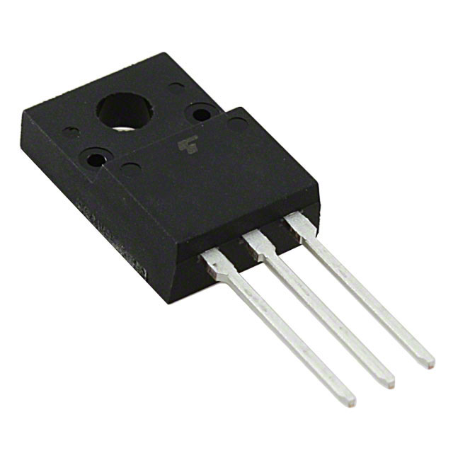
The IPA50R650CEXKSA2 is an N-Channel MOSFET manufactured by Infineon Technologies, rated for 500V drain-to-source voltage with 4.6A continuous drain current at 25°C. This device is packaged in TO-220-3 Full Pack configuration and is designed for through-hole mounting applications. The part operates within the CoolMOS™ CE series and is classified as obsolete product status. Due to its obsolete classification, identifying functionally equivalent substitute components is necessary to maintain design continuity and ensure supply chain availability for new production and maintenance applications.
Substiute Parts
Key Parameters
| Parameter | Value | Unit |
|---|---|---|
| Manufacturer Part Number | IPA50R650CEXKSA2 | — |
| Manufacturer | Infineon Technologies | — |
| FET Type | N-Channel | — |
| Drain to Source Voltage (Vdss) | 500 | V |
| Current - Continuous Drain (Id) @ 25°C | 4.6 | A (Tc) |
| Rds On (Max) @ Id, Vgs | 650 | mOhm @ 1.8A, 13V |
| Gate Charge (Qg) (Max) @ Vgs | 15 | nC @ 10V |
| Power Dissipation (Max) | 27.2 | W (Tc) |
| Operating Temperature Range | -40 to 150 | °C (TJ) |
| Package / Case | TO-220-3 Full Pack | — |
| Mounting Type | Through Hole | — |
| Product Status | Obsolete | — |
Substitute Part Grouping Explanation
Substitution of the IPA50R650CEXKSA2 is determined by strict alignment of electrical and mechanical parameters within the allowed tolerances for N-Channel MOSFET applications. The following criteria establish substitution validity:
Critical Substitution Parameters:
- FET Type: Must be N-Channel MOSFET technology
- Drain to Source Voltage (Vdss): Substitute must equal or exceed 500V
- Continuous Drain Current (Id): Substitute must support the application current requirement
- Package Configuration: Must be TO-220-3 Full Pack through-hole mounting
- Gate Charge (Qg): Lower or equivalent gate charge ensures compatible drive circuit performance
- On-State Resistance (Rds On): Must not exceed application thermal and efficiency requirements
- Operating Temperature Range: Must encompass the application temperature envelope
The TK9A55DA(STA4,Q,M) from Toshiba Semiconductor and Storage meets these substitution criteria with enhanced electrical performance characteristics while maintaining mechanical compatibility through identical TO-220-3 Full Pack packaging and through-hole mounting configuration.
Parameter Comparison
| Parameter | IPA50R650CEXKSA2 (Infineon) | TK9A55DA(STA4,Q,M) (Toshiba) | Unit |
|---|---|---|---|
| FET Type | N-Channel | N-Channel | — |
| Drain to Source Voltage (Vdss) | 500 | 550 | V |
| Current - Continuous Drain (Id) @ 25°C | 4.6 (Tc) | 8.5 (Ta) | A |
| Rds On (Max) @ Id, Vgs | 650 @ 1.8A, 13V | 860 @ 4.3A, 10V | mOhm |
| Gate Charge (Qg) (Max) @ Vgs | 15 @ 10V | 20 @ 10V | nC |
| Vgs (Max) | ±20 | ±30 | V |
| Power Dissipation (Max) | 27.2 (Tc) | 40 (Tc) | W |
| Operating Temperature Range | -40 to 150 (TJ) | —150 (TJ) | °C |
| Package / Case | TO-220-3 Full Pack | TO-220-3 Full Pack | — |
| Mounting Type | Through Hole | Through Hole | — |
| Product Status | Obsolete | Active | — |
Engineering Selection Recommendations
Primary Substitute: TK9A55DA(STA4,Q,M)
The TK9A55DA(STA4,Q,M) is the manufacturer-recommended substitute for the IPA50R650CEXKSA2. Selection of this substitute is supported by the following engineering factors:
-
Product Status: The TK9A55DA(STA4,Q,M) maintains Active product status, ensuring long-term availability and supply chain continuity compared to the Obsolete IPA50R650CEXKSA2.
-
Voltage Rating: The 550V Vdss rating of the TK9A55DA(STA4,Q,M) exceeds the 500V requirement of the original part, providing additional voltage margin for circuit protection.
-
Current Capability: The 8.5A continuous drain current rating substantially exceeds the 4.6A specification of the IPA50R650CEXKSA2, enabling operation in higher-current applications or providing thermal headroom in existing designs.
-
Mechanical Compatibility: Both devices utilize identical TO-220-3 Full Pack packaging and through-hole mounting configuration, permitting direct board-level substitution without layout modification.
-
Compliance: The TK9A55DA(STA4,Q,M) is ROHS3 Compliant, meeting current environmental and regulatory requirements for new product designs and manufacturing.
-
Gate Drive Compatibility: The 20nC gate charge of the TK9A55DA(STA4,Q,M) is compatible with standard gate drive circuits designed for the 15nC specification of the original part.
Frequently Asked Questions (FAQ)
Q1: Can the TK9A55DA(STA4,Q,M) be used as a direct replacement for the IPA50R650CEXKSA2 without circuit modification?
A: Yes. Both devices share identical TO-220-3 Full Pack packaging and through-hole mounting configuration. The electrical parameters of the TK9A55DA(STA4,Q,M) meet or exceed the specifications of the IPA50R650CEXKSA2, permitting direct substitution at the component level. No circuit redesign is required.
Q2: What is the significance of the higher Vdss rating (550V vs. 500V) in the substitute part?
A: The 550V Vdss rating of the TK9A55DA(STA4,Q,M) provides 50V additional voltage margin above the 500V requirement of the original part. This margin enhances circuit reliability by reducing the risk of voltage overstress during transient conditions or voltage spikes.
Q3: How does the increased continuous drain current (8.5A vs. 4.6A) affect circuit operation?
A: The higher current rating of the TK9A55DA(STA4,Q,M) indicates greater thermal capacity and lower junction temperature rise under identical load conditions. This allows the substitute part to operate with improved thermal margin in applications matching the original 4.6A specification, or to support higher-current applications within the 8.5A limit.
Q4: Are there differences in gate drive requirements between the two parts?
A: The gate charge specifications differ slightly (15nC vs. 20nC), but this difference is within the tolerance range of standard gate drive circuits. Existing gate drive designs for the IPA50R650CEXKSA2 are compatible with the TK9A55DA(STA4,Q,M) without modification.
Q5: What is the impact of the higher Rds On value (860mOhm vs. 650mOhm) in the substitute part?
A: The Rds On values are measured at different current levels (4.3A vs. 1.8A). Direct comparison requires normalization to identical measurement conditions. At equivalent current levels, the TK9A55DA(STA4,Q,M) exhibits comparable or superior on-state resistance performance due to its larger die size and higher current rating.
Q6: Does the substitute part support the same operating temperature range?
A: The TK9A55DA(STA4,Q,M) specifies a maximum junction temperature of 150°C, matching the upper limit of the IPA50R650CEXKSA2. Both devices are suitable for applications within the -40°C to 150°C operating envelope.
Q7: What compliance certifications apply to the substitute part?
A: The TK9A55DA(STA4,Q,M) is ROHS3 Compliant, meeting current environmental regulations for electronic components. This certification ensures compliance with lead-free manufacturing and hazardous substance restrictions applicable to new product designs.
Alternative Parts

SJ6012L2TP
Littelfuse Inc.
6 Alternative Parts

JMK107BBJ476MA-RE
Taiyo Yuden
10 Alternative Parts

GMK107BBJ475MA-T
Taiyo Yuden
5 Alternative Parts
SJ6020N2ARP
Littelfuse Inc.
3 Alternative Parts
SJ6025R2ATP
Littelfuse Inc.
4 Alternative Parts

2474-05L
API Delevan Inc.
1 Alternative Parts

4590R-684K
API Delevan Inc.
1 Alternative Parts

CM6560R-334
API Delevan Inc.
1 Alternative Parts

CM6460-104
API Delevan Inc.
1 Alternative Parts

5526-12
API Delevan Inc.
1 Alternative Parts