


Request Quote
(Ships tomorrow)
INA114AP Instrumentation Amplifier Equivalent & Substitute Parts
Part Overview
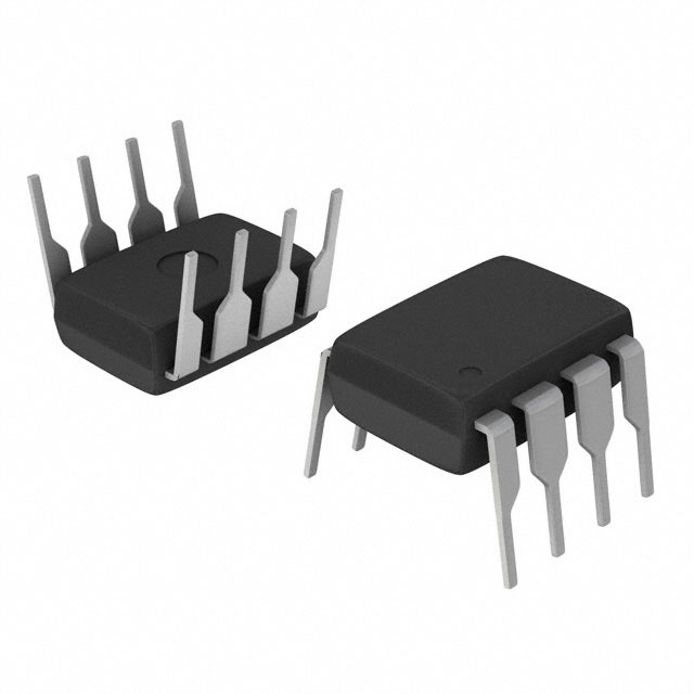
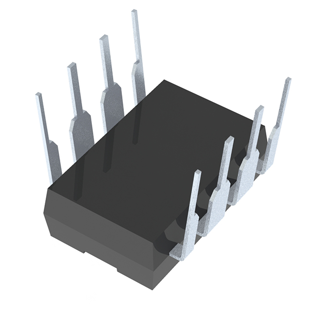
The INA114AP is a single-circuit instrumentation amplifier manufactured by Texas Instruments in 8-PDIP through-hole packaging. This device is classified as an active linear amplifier with an operating temperature range of -40°C to 85°C and is currently in active product status. The INA114AP is widely used in precision signal conditioning applications requiring low input bias current and low input offset voltage. Equivalent and substitute parts are identified based on matching electrical performance parameters, mechanical compatibility, and functional equivalence within the instrumentation amplifier category.
Substiute Parts
Key Parameters
| Parameter | INA114AP Value | Unit | Substitution Relevance |
|---|---|---|---|
| Amplifier Type | Instrumentation | — | Core functional classification |
| Number of Circuits | 1 | — | Channel count must match |
| Slew Rate | 0.6 | V/µs | Signal response speed |
| -3dB Bandwidth | 1 | MHz | Frequency response specification |
| Current - Input Bias | 500 | pA | Input impedance characteristic |
| Voltage - Input Offset | 25 | µV | DC accuracy specification |
| Current - Supply | 2.2 | mA | Power consumption |
| Current - Output / Channel | 20 | mA | Output drive capability |
| Voltage - Supply Span (Min) | 4.5 | V | Minimum operating voltage |
| Voltage - Supply Span (Max) | 36 | V | Maximum operating voltage |
| Operating Temperature | -40 to 85 | °C | Environmental operating range |
| Package / Case | 8-DIP (0.300", 7.62mm) | — | Physical and electrical compatibility |
| Mounting Type | Through Hole | — | PCB assembly method |
| RoHS Status | ROHS3 Compliant | — | Environmental compliance |
Substitute Part Grouping Explanation
Substitution of the INA114AP is determined by strict alignment of electrical and mechanical parameters. The following criteria establish valid substitution relationships:
Primary Substitution Criteria:
- Amplifier Type: Must be Instrumentation
- Number of Circuits: Must equal 1
- Package / Case: Must be 8-DIP (0.300", 7.62mm)
- Mounting Type: Must be Through Hole
- Operating Temperature Range: Must encompass or match -40°C to 85°C
- Voltage Supply Span: Must support 4.5V minimum to 36V maximum range
- RoHS Status: Must be ROHS3 Compliant
Secondary Performance Parameters (Allowable Variation):
- Slew Rate: 0.6 V/µs baseline; higher values acceptable
- -3dB Bandwidth: 1 MHz baseline; equal or higher acceptable
- Current - Input Bias: 500 pA baseline; lower values acceptable
- Voltage - Input Offset: 25 µV baseline; lower values acceptable
- Current - Supply: 2.2 mA baseline; lower values preferred
- Current - Output / Channel: 20 mA baseline; equal or higher acceptable
Substitute parts are grouped into two categories: direct equivalents from Analog Devices Inc. (AD620 and AD621 series) and compatible alternatives (AMP02 and LT1167/LT1168/LT1920 series) that meet all primary criteria with enhanced or comparable secondary performance.
Parameter Comparison
| Parameter | INA114AP | AD620ANZ | AD620BNZ | AD621ANZ | AD622ANZ | AMP02EPZ | AMP02FPZ | LT1167CN8#PBF | LT1167IN8#PBF | LT1168ACN8#PBF | LT1920CN8#PBF |
|---|---|---|---|---|---|---|---|---|---|---|---|
| Manufacturer | Texas Instruments | Analog Devices | Analog Devices | Analog Devices | Analog Devices | Analog Devices | Analog Devices | Analog Devices | Analog Devices | Analog Devices | Analog Devices |
| Amplifier Type | Instrumentation | Instrumentation | Instrumentation | Instrumentation | Instrumentation | Instrumentation | Instrumentation | Instrumentation | Instrumentation | Instrumentation | Instrumentation |
| Number of Circuits | 1 | 1 | 1 | 1 | 1 | 1 | 1 | 1 | 1 | 1 | 1 |
| Slew Rate (V/µs) | 0.6 | 1.2 | 1.2 | 1.2 | 1.2 | 6 | 6 | 1.2 | 1.2 | 0.5 | 1.2 |
| -3dB Bandwidth / Gain Bandwidth Product (MHz / kHz) | 1 MHz | 1 MHz | 1 MHz | 800 kHz | 1 MHz | 1.2 MHz | 1.2 MHz | 1 MHz | 1 MHz | 400 kHz | 1 MHz |
| Current - Input Bias (pA / nA) | 500 pA | 500 pA | 500 pA | 500 pA | 2 nA | 2 nA | 4 nA | 80 pA | 80 pA | 40 pA | 500 pA |
| Voltage - Input Offset (µV) | 25 | 30 | 15 | 75 | 60 | 20 | 40 | 20 | 20 | 15 | 30 |
| Current - Supply (mA / µA) | 2.2 | 0.9 | 0.9 | 0.9 | 0.9 | 5 | 5 | 0.9 | 0.9 | 0.35 | 0.9 |
| Current - Output / Channel (mA) | 20 | 18 | 18 | 18 | 18 | 32 | 32 | — | 27 | 32 | — |
| Voltage - Supply Span Min (V) | 4.5 | 4.6 | 4.6 | 4.6 | 5.2 | 9 | 9 | 4.6 | 4.6 | 4.6 | 4.6 |
| Voltage - Supply Span Max (V) | 36 | 36 | 36 | 36 | 36 | 36 | 36 | 36 | 36 | 36 | 36 |
| Operating Temperature (°C) | -40 to 85 | -40 to 85 | -40 to 85 | -40 to 85 | -40 to 85 | -40 to 85 | -40 to 85 | 0 to 70 | -40 to 85 | 0 to 70 | 0 to 70 |
| Package / Case | 8-DIP (0.300", 7.62mm) | 8-DIP (0.300", 7.62mm) | 8-DIP (0.300", 7.62mm) | 8-DIP (0.300", 7.62mm) | 8-DIP (0.300", 7.62mm) | 8-DIP (0.300", 7.62mm) | 8-DIP (0.300", 7.62mm) | 8-DIP (0.300", 7.62mm) | 8-DIP (0.300", 7.62mm) | 8-DIP (0.300", 7.62mm) | 8-DIP (0.300", 7.62mm) |
| Mounting Type | Through Hole | Through Hole | Through Hole | Through Hole | Through Hole | Through Hole | Through Hole | Through Hole | Through Hole | Through Hole | Through Hole |
| RoHS Status | ROHS3 Compliant | ROHS3 Compliant | ROHS3 Compliant | ROHS3 Compliant | ROHS3 Compliant | ROHS3 Compliant | ROHS3 Compliant | ROHS3 Compliant | ROHS3 Compliant | ROHS3 Compliant | ROHS3 Compliant |
Engineering Selection Recommendations
Primary Substitutes (Recommended for Direct Replacement):
AD620ANZ and AD620BNZ are the primary recommended substitutes for the INA114AP. Both devices maintain full compatibility across all primary substitution criteria. The AD620BNZ offers superior input offset voltage performance (15 µV versus 25 µV) while maintaining identical supply voltage range and operating temperature specifications. Both AD620 variants feature reduced supply current (0.9 mA versus 2.2 mA), resulting in lower power consumption. These devices are manufactured by Analog Devices Inc. and carry ROHS3 compliance with unlimited moisture sensitivity level rating.
Secondary Substitutes (Compatible with Performance Trade-offs):
AD621ANZ provides instrumentation amplifier functionality with reduced -3dB bandwidth (800 kHz versus 1 MHz) but maintains all primary mechanical and electrical compatibility parameters. This device is suitable for applications where bandwidth reduction is acceptable.
AD622ANZ introduces higher input bias current (2 nA versus 500 pA) and requires minimum supply voltage of 5.2V (versus 4.5V for INA114AP). This device is compatible only in systems with supply voltages at or above 5.2V.
AMP02EPZ and AMP02FPZ feature significantly higher slew rate (6 V/µs versus 0.6 V/µs) and bandwidth (1.2 MHz versus 1 MHz), with higher output current capability (32 mA versus 20 mA). However, these devices require minimum supply voltage of 9V, restricting use to higher-voltage systems. Input bias current is 2 nA to 4 nA, higher than the INA114AP baseline.
Specialized Substitutes (Limited Compatibility):
LT1167CN8#PBF and LT1167IN8#PBF are compatible substitutes with lower input bias current (80 pA) and input offset voltage (20 µV). LT1167CN8#PBF operates within 0°C to 70°C temperature range, limiting use in applications requiring full -40°C to 85°C operation. LT1167IN8#PBF supports the full -40°C to 85°C range and is suitable for extended-temperature applications.
LT1168ACN8#PBF features the lowest supply current (0.35 mA) and reduced slew rate (0.5 V/µs), with operating temperature limited to 0°C to 70°C. This device is appropriate for low-power applications within the restricted temperature range.
LT1920CN8#PBF maintains 1 MHz bandwidth and 1.2 V/µs slew rate with operating temperature limited to 0°C to 70°C. This device is suitable for standard-performance applications within the restricted temperature range.
Compliance and Certification:
All substitute parts listed carry ROHS3 compliance and REACH Unaffected status, matching the environmental compliance profile of the INA114AP. All devices are classified as active products with current manufacturing status.
Frequently Asked Questions (FAQ)
Q: Can AD620ANZ be used as a direct replacement for INA114AP in all applications?
A: AD620ANZ meets all primary substitution criteria including package type, mounting method, operating temperature range, and supply voltage specifications. The device is pin-compatible and functionally equivalent. However, AD620ANZ features lower supply current (0.9 mA versus 2.2 mA) and higher slew rate (1.2 V/µs versus 0.6 V/µs), which may affect circuit behavior in applications with specific power budget or signal response requirements. Verification of circuit performance is necessary when substituting in precision applications.
Q: What is the key difference between AD620BNZ and AD620ANZ?
A: Both devices are functionally equivalent with identical electrical specifications except for input offset voltage. AD620BNZ specifies 15 µV input offset voltage compared to 30 µV for AD620ANZ. For applications requiring lower DC offset error, AD620BNZ is the preferred selection. Both devices maintain identical supply current, bandwidth, and temperature range specifications.
Q: Why do AMP02EPZ and AMP02FPZ require 9V minimum supply voltage while INA114AP operates at 4.5V?
A: AMP02 series devices feature higher performance specifications including 6 V/µs slew rate and 1.2 MHz bandwidth, requiring higher internal bias voltages for operation. This design trade-off results in the 9V minimum supply requirement. These devices are suitable only for systems with supply voltages at or above 9V. For low-voltage applications, AD620 or LT1167 series devices are appropriate alternatives.
Q: Are LT1167CN8#PBF and LT1167IN8#PBF interchangeable?
A: Both devices are functionally identical with matching electrical specifications. The primary difference is operating temperature range: LT1167CN8#PBF operates 0°C to 70°C while LT1167IN8#PBF operates -40°C to 85°C. Selection depends on application temperature requirements. For applications requiring full military or extended-temperature operation, LT1167IN8#PBF is required. For standard commercial temperature range applications, either device is acceptable.
Q: What is the significance of the 8-DIP package specification for substitution?
A: The 8-DIP (0.300", 7.62mm) package specification ensures mechanical and electrical pin compatibility. All listed substitute parts use identical package dimensions and pin assignments, allowing direct PCB socket replacement without layout modification. Package compatibility is a mandatory substitution criterion for through-hole mounted instrumentation amplifiers.
Q: Can LT1168ACN8#PBF be used in applications requiring -40°C operation?
A: No. LT1168ACN8#PBF specifies operating temperature range of 0°C to 70°C and is not rated for operation below 0°C. Applications requiring -40°C minimum operating temperature must use devices with -40°C to 85°C specifications, such as AD620ANZ, AD620BNZ, AD621ANZ, AD622ANZ, AMP02EPZ, AMP02FPZ, or LT1167IN8#PBF.
Q: What does ROHS3 Compliant status indicate for component selection?
A: ROHS3 Compliant status indicates the device meets Restriction of Hazardous Substances Directive requirements, restricting use of lead, cadmium, mercury, and other hazardous materials. All listed substitute parts carry identical ROHS3 compliance, ensuring compatibility with environmental regulations and procurement requirements matching the INA114AP specification.
Q: Is input bias current reduction from 500 pA to 80 pA (LT1167 series) significant for circuit design?
A: Input bias current affects circuit accuracy in high-impedance signal conditioning applications. Lower input bias current reduces error voltage across high-impedance sources. LT1167 series devices with 80 pA input bias current provide improved performance in applications with source impedances exceeding 1 MΩ. For standard applications with source impedances below 100 kΩ, the difference is negligible.
Alternative Parts

SJ6012L2TP
Littelfuse Inc.
6 Alternative Parts

JMK107BBJ476MA-RE
Taiyo Yuden
10 Alternative Parts

GMK107BBJ475MA-T
Taiyo Yuden
5 Alternative Parts
SJ6020N2ARP
Littelfuse Inc.
3 Alternative Parts
SJ6025R2ATP
Littelfuse Inc.
4 Alternative Parts

2474-05L
API Delevan Inc.
1 Alternative Parts

4590R-684K
API Delevan Inc.
1 Alternative Parts

CM6560R-334
API Delevan Inc.
1 Alternative Parts

CM6460-104
API Delevan Inc.
1 Alternative Parts

5526-12
API Delevan Inc.
1 Alternative Parts