


Request Quote
(Ships tomorrow)
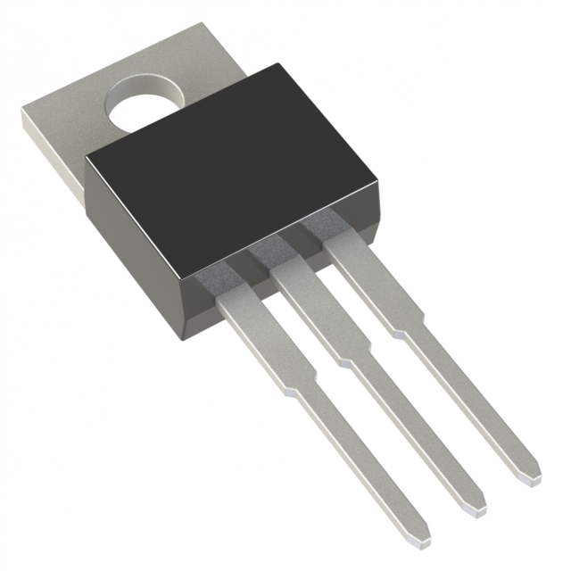
FQP3N90 Equivalent & Substitute Parts
Part Overview
The FQP3N90 is an N-Channel MOSFET manufactured by onsemi, rated for 900V drain-to-source voltage with 3.6A continuous drain current at 25°C. This device is packaged in a Through Hole TO-220-3 configuration and is part of the QFET® series. The FQP3N90 is classified as obsolete, making identification of equivalent and substitute parts necessary for ongoing design support and procurement continuity. Substitute parts must maintain compatibility across electrical ratings, thermal characteristics, and mechanical packaging to ensure direct replacement capability in existing applications.
Substiute Parts
Key Parameters
| Parameter | FQP3N90 | Unit |
|---|---|---|
| Drain to Source Voltage (Vdss) | 900 | V |
| Continuous Drain Current (Id) @ 25°C | 3.6 | A |
| Rds On (Max) @ Id, Vgs | 4.25 @ 1.8A, 10V | Ohm |
| Gate Threshold Voltage (Vgs(th)) @ Id | 5 @ 250µA | V |
| Gate Charge (Qg) @ Vgs | 26 @ 10V | nC |
| Power Dissipation (Max) | 130 | W |
| Operating Temperature Range | -55 to 150 | °C |
| Package Type | TO-220-3 | — |
| Mounting Type | Through Hole | — |
| FET Type | N-Channel | — |
| Technology | MOSFET (Metal Oxide) | — |
Substitute Part Grouping Explanation
Substitute parts for the FQP3N90 are selected based on the following critical parameters that determine functional equivalence:
Primary Compatibility Criteria:
- FET Type: N-Channel (all substitutes must be N-Channel)
- Technology: MOSFET (Metal Oxide)
- Package/Case: TO-220-3 (Through Hole mounting)
- Drain to Source Voltage (Vdss): 900V or higher
- Continuous Drain Current (Id): 3.6A or higher at 25°C
- Operating Temperature Range: -55°C to 150°C or wider
- Drive Voltage: 10V gate drive compatibility
Substitution Logic: Parts are grouped as equivalent when they meet or exceed the electrical performance specifications of the FQP3N90 while maintaining identical or compatible package configurations. Vdss ratings equal to or greater than 900V are acceptable. Continuous drain current ratings at or above 3.6A ensure thermal and current-handling capability. Gate charge, threshold voltage, and on-resistance characteristics must remain within acceptable ranges to prevent circuit performance degradation.
Parameter Comparison
| Parameter | FQP3N90 (onsemi) | STP3NK90Z (STMicroelectronics) | IXTP3N100P (IXYS) | Unit |
|---|---|---|---|---|
| Drain to Source Voltage (Vdss) | 900 | 900 | 1000 | V |
| Continuous Drain Current (Id) @ 25°C | 3.6 | 3.0 | 3.0 | A |
| Rds On (Max) @ Id, Vgs | 4.25 @ 1.8A, 10V | 4.8 @ 1.5A, 10V | 4.8 @ 1.5A, 10V | Ohm |
| Gate Threshold Voltage (Vgs(th)) @ Id | 5 @ 250µA | 4.5 @ 50µA | 4.5 @ 250µA | V |
| Gate Charge (Qg) @ Vgs | 26 @ 10V | 22.7 @ 10V | 39 @ 10V | nC |
| Input Capacitance (Ciss) @ Vds | 910 @ 25V | 590 @ 25V | 1100 @ 25V | pF |
| Power Dissipation (Max) | 130 | 90 | 125 | W |
| Operating Temperature Range | -55 to 150 | -55 to 150 | -55 to 150 | °C |
| Package Type | TO-220-3 | TO-220-3 | TO-220-3 | — |
| FET Type | N-Channel | N-Channel | N-Channel | — |
| Technology | MOSFET (Metal Oxide) | MOSFET (Metal Oxide) | MOSFET (Metal Oxide) | — |
Engineering Selection Recommendations
STP3NK90Z (STMicroelectronics): The STP3NK90Z is an active product with RoHS3 compliance and is recommended as the primary substitute for the obsolete FQP3N90. Both devices share identical 900V Vdss ratings and TO-220-3 packaging. The STP3NK90Z operates within the same temperature range and maintains REACH compliance. The continuous drain current rating of 3.0A is lower than the FQP3N90's 3.6A specification; however, this device is suitable for applications where the circuit design accommodates the reduced current rating. Gate charge is lower (22.7 nC versus 26 nC), resulting in improved switching efficiency. Power dissipation is rated at 90W compared to 130W for the FQP3N90, requiring thermal design verification for high-power applications.
IXTP3N100P (IXYS): The IXTP3N100P is an active product with RoHS3 compliance and represents an alternative substitute option. This device features a higher Vdss rating of 1000V, providing additional voltage margin over the FQP3N90. The continuous drain current is 3.0A, matching the STP3NK90Z. The IXTP3N100P exhibits higher gate charge (39 nC) and input capacitance (1100 pF) compared to the FQP3N90, which may impact switching speed and gate drive requirements. Power dissipation is rated at 125W, closer to the FQP3N90's 130W specification. This device is suitable for applications requiring higher voltage headroom.
Product Status Consideration: Both substitute parts are classified as active products, ensuring long-term availability and supply chain stability compared to the obsolete FQP3N90. Selection between STP3NK90Z and IXTP3N100P depends on specific application requirements regarding voltage margin, current capacity, and thermal management.
Frequently Asked Questions (FAQ)
Q: Can the STP3NK90Z directly replace the FQP3N90 in all applications?
A: The STP3NK90Z is mechanically and electrically compatible with the FQP3N90 in terms of package type (TO-220-3) and voltage rating (900V). However, the continuous drain current is reduced from 3.6A to 3.0A. Direct replacement is possible only in applications where the circuit design operates at or below 3.0A continuous drain current. Thermal design verification is required due to the lower power dissipation rating (90W versus 130W).
Q: What is the difference between the STP3NK90Z and IXTP3N100P?
A: Both devices are active N-Channel MOSFETs in TO-220-3 packages with identical continuous drain current ratings (3.0A). The primary differences are: (1) Vdss rating—STP3NK90Z is 900V, IXTP3N100P is 1000V; (2) Gate charge—STP3NK90Z is 22.7 nC, IXTP3N100P is 39 nC; (3) Input capacitance—STP3NK90Z is 590 pF, IXTP3N100P is 1100 pF; (4) Power dissipation—STP3NK90Z is 90W, IXTP3N100P is 125W. Selection depends on whether higher voltage margin or lower switching losses are prioritized.
Q: Are there any compliance or regulatory differences between the FQP3N90 and its substitutes?
A: All three devices (FQP3N90, STP3NK90Z, and IXTP3N100P) share identical REACH compliance status (REACH Unaffected) and ECCN classification (EAR99). The STP3NK90Z and IXTP3N100P are RoHS3 compliant, whereas the FQP3N90 does not specify RoHS status. All devices have Moisture Sensitivity Level 1 (Unlimited), indicating no moisture sensitivity concerns.
Q: What is the impact of higher gate charge in the IXTP3N100P?
A: The IXTP3N100P has a gate charge of 39 nC compared to 26 nC for the FQP3N90. Higher gate charge requires more energy to switch the device and may necessitate gate driver adjustments to maintain switching speed. This characteristic is relevant in high-frequency switching applications where gate drive power consumption and switching losses are critical design parameters.
Q: Can I use the IXTP3N100P in a circuit designed for 900V operation?
A: Yes. The IXTP3N100P is rated for 1000V Vdss, which exceeds the 900V requirement. This provides additional voltage margin and is suitable for 900V applications. However, the higher input capacitance (1100 pF versus 910 pF) may affect circuit behavior in high-frequency or high-impedance gate drive circuits.
Q: What thermal considerations apply when substituting the FQP3N90?
A: The FQP3N90 is rated for 130W power dissipation. The STP3NK90Z is rated for 90W and the IXTP3N100P for 125W. If the original circuit design relies on the 130W dissipation capability, thermal analysis is required to confirm that the substitute device's lower rating does not cause excessive junction temperature rise. Heatsink design may require adjustment.
Alternative Parts

SJ6012L2TP
Littelfuse Inc.
6 Alternative Parts

JMK107BBJ476MA-RE
Taiyo Yuden
10 Alternative Parts

GMK107BBJ475MA-T
Taiyo Yuden
5 Alternative Parts
SJ6020N2ARP
Littelfuse Inc.
3 Alternative Parts
SJ6025R2ATP
Littelfuse Inc.
4 Alternative Parts

2474-05L
API Delevan Inc.
1 Alternative Parts

4590R-684K
API Delevan Inc.
1 Alternative Parts

CM6560R-334
API Delevan Inc.
1 Alternative Parts

CM6460-104
API Delevan Inc.
1 Alternative Parts

5526-12
API Delevan Inc.
1 Alternative Parts