


Request Quote
(Ships tomorrow)
FQD6N50CTF Equivalent & Substitute Parts
Part Overview
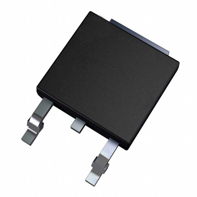
The FQD6N50CTF is an N-Channel MOSFET manufactured by onsemi, rated for 500V drain-to-source voltage with 4.5A continuous drain current. The device is packaged in TO-252-3 (DPAK) surface mount configuration and is designed for high-voltage switching applications. The FQD6N50CTF is classified as obsolete, making identification of equivalent and substitute parts necessary for ongoing design support and production continuity. Substitute parts must maintain electrical compatibility across voltage, current, and thermal specifications while accommodating the same or compatible package footprints.
Substiute Parts
Key Parameters
| Parameter | Value | Unit |
|---|---|---|
| Drain-to-Source Voltage (Vdss) | 500 | V |
| Continuous Drain Current (Id) @ 25°C | 4.5 | A |
| On-State Resistance (Rds On) @ Id, Vgs | 1.2 @ 2.25A, 10V | Ohm |
| Gate Threshold Voltage (Vgs(th)) @ Id | 4 | V @ 250µA |
| Gate Charge (Qg) @ Vgs | 25 | nC @ 10V |
| Maximum Gate Voltage (Vgs) | ±30 | V |
| Input Capacitance (Ciss) @ Vds | 700 | pF @ 25V |
| Power Dissipation (Max) | 2.5 (Ta), 61 (Tc) | W |
| Operating Temperature Range | -55 to 150 | °C (TJ) |
| Package Type | TO-252-3, DPAK | Surface Mount |
| Moisture Sensitivity Level | 1 (Unlimited) | MSL |
Substitute Part Grouping Explanation
Substitution of the FQD6N50CTF is determined by the following critical electrical and mechanical parameters:
Voltage Rating Compatibility: All substitute parts must maintain a minimum Vdss rating of 500V to ensure safe operation in the original application circuit. Parts with higher voltage ratings (525V) are acceptable as they provide additional design margin.
Current Rating Compatibility: The continuous drain current (Id) must be equal to or greater than 4.5A to support the original application load requirements. Substitute parts rated at 4.4A, 5A, or 6A satisfy this criterion.
On-State Resistance (Rds On): The maximum on-state resistance at specified gate and drain conditions must not significantly exceed the original specification (1.2 Ohm @ 2.25A, 10V) to prevent excessive power dissipation and thermal stress. Acceptable substitutes show Rds On values between 1.2 and 1.5 Ohm under comparable test conditions.
Package Compatibility: All substitute parts must use the TO-252-3 DPAK surface mount package to ensure mechanical and electrical compatibility with existing PCB layouts and assembly processes.
Gate Charge (Qg): Gate charge values between 12 and 28 nC are acceptable, as these variations do not materially affect switching performance in typical applications.
Operating Temperature Range: Substitute parts must support the full operating temperature range of -55°C to 150°C (TJ) or equivalent.
Product Status and Compliance: Active product status is preferred for long-term availability. RoHS3 compliance and REACH unaffected status are standard for modern substitutes.
Parameter Comparison
| Parameter | FQD6N50CTF (onsemi) | RJK5033DPD-00#J2 (Renesas) | STD5NK50ZT4 (STMicroelectronics) | STD6N52K3 (STMicroelectronics) | TK6P53D(T6RSS-Q) (Toshiba) |
|---|---|---|---|---|---|
| Vdss (V) | 500 | 500 | 500 | 525 | 525 |
| Id @ 25°C (A) | 4.5 (Tc) | 6 (Ta) | 4.4 (Tc) | 5 (Tc) | 6 (Ta) |
| Rds On (Ohm) | 1.2 @ 2.25A, 10V | 1.3 @ 3A, 10V | 1.5 @ 2.2A, 10V | 1.2 @ 2.5A, 10V | 1.3 @ 3A, 10V |
| Vgs(th) (V) | 4 @ 250µA | Not specified | 4.5 @ 50µA | 4.5 @ 100µA | 4.4 @ 1mA |
| Qg (nC) | 25 @ 10V | Not specified | 28 @ 10V | Not specified | 12 @ 10V |
| Ciss (pF) | 700 @ 25V | 600 @ 25V | 535 @ 25V | Not specified | 600 @ 25V |
| Power Dissipation (W) | 2.5 (Ta), 61 (Tc) | 65 (Tc) | 70 (Tc) | 70 (Tc) | 100 (Tc) |
| Operating Temperature (°C) | -55 to 150 | 150 (TJ) | -55 to 150 | 150 (TJ) | 150 (TJ) |
| Package | TO-252-3, DPAK | TO-252-3, DPAK | TO-252-3, DPAK | TO-252-3, DPAK | TO-252-3, DPAK |
| Product Status | Obsolete | Active | Active | Active | Active |
| RoHS Status | Not specified | ROHS3 Compliant | ROHS3 Compliant | ROHS3 Compliant | ROHS3 Compliant |
Engineering Selection Recommendations
Primary Substitute: STD6N52K3 (STMicroelectronics)
The STD6N52K3 provides the closest electrical match to the FQD6N50CTF. It maintains identical on-state resistance (1.2 Ohm @ 2.5A, 10V), supports 5A continuous drain current, and offers a 525V voltage rating that exceeds the original specification. The device is active in production, RoHS3 compliant, and available in the same TO-252-3 DPAK package. The higher voltage rating provides additional design margin for transient overvoltage conditions.
Secondary Substitute: STD5NK50ZT4 (STMicroelectronics)
The STD5NK50ZT4 matches the original 500V voltage rating and 4.4A current rating, providing near-identical electrical performance. On-state resistance is slightly elevated at 1.5 Ohm but remains within acceptable limits for most applications. This device is active, RoHS3 compliant, and widely available. The SuperMESH™ technology provides enhanced switching characteristics.
Alternative Substitute: RJK5033DPD-00#J2 (Renesas Electronics Corporation)
The RJK5033DPD-00#J2 offers higher current capability (6A) and improved power dissipation (65W Tc) compared to the original part. The 500V voltage rating and 1.3 Ohm on-state resistance provide direct electrical compatibility. This device is active and available in high inventory quantities. Packaging is specified as MP-3A, which is mechanically compatible with TO-252-3 DPAK footprints.
Alternative Substitute: TK6P53D(T6RSS-Q) (Toshiba Semiconductor and Storage)
The TK6P53D(T6RSS-Q) provides the highest performance specifications among available substitutes, with 6A current rating, 525V voltage rating, and 100W power dissipation capability. Gate charge is optimized at 12 nC, enabling faster switching transitions. The device is active, RoHS3 compliant, and uses the π-MOSVII technology platform. This part is suitable for applications requiring enhanced thermal performance.
All substitute parts are classified as active products with current manufacturing status, ensuring long-term availability and supply chain stability. All recommended substitutes comply with RoHS3 and REACH requirements, meeting modern environmental and regulatory standards.
Frequently Asked Questions (FAQ)
Q: Can the STD6N52K3 be used as a direct replacement for the FQD6N50CTF?
A: Yes. The STD6N52K3 provides direct electrical and mechanical compatibility. Both devices share identical on-state resistance (1.2 Ohm), support equivalent current ratings (5A vs. 4.5A), and use the same TO-252-3 DPAK package. The 525V rating of the STD6N52K3 exceeds the 500V requirement, providing additional voltage margin. No circuit modifications are required.
Q: What is the primary difference between the RJK5033DPD-00#J2 and STD5NK50ZT4?
A: The RJK5033DPD-00#J2 (Renesas) offers higher current capability (6A vs. 4.4A) and lower on-state resistance (1.3 Ohm vs. 1.5 Ohm), resulting in superior thermal performance. The STD5NK50ZT4 (STMicroelectronics) maintains closer alignment to the original 4.5A current specification and uses SuperMESH™ technology. Selection depends on whether the application requires higher current headroom or closer parameter matching.
Q: Are all substitute parts available in the same package as the FQD6N50CTF?
A: Yes. All listed substitute parts use the TO-252-3 DPAK surface mount package, ensuring mechanical compatibility with existing PCB layouts. The RJK5033DPD-00#J2 specifies MP-3A packaging, which is electrically and mechanically equivalent to TO-252-3 DPAK for this device category.
Q: Why is the TK6P53D(T6RSS-Q) rated for higher power dissipation than the original part?
A: The TK6P53D(T6RSS-Q) achieves 100W power dissipation (Tc) compared to 61W (Tc) for the FQD6N50CTF due to improved semiconductor design and lower on-state resistance. Higher power dissipation capability indicates better thermal performance and lower junction temperature rise under identical load conditions. This enhancement does not affect compatibility; it provides additional design margin.
Q: What is the significance of the gate charge (Qg) differences among substitute parts?
A: Gate charge values range from 12 nC (TK6P53D) to 28 nC (STD5NK50ZT4). Lower gate charge enables faster switching transitions and reduced driver power consumption. Higher gate charge requires longer switching times but does not affect DC operating characteristics. Selection should consider the gate driver circuit specifications and switching frequency requirements of the application.
Q: Can the FQD6N50CTF be replaced with a part rated for lower voltage, such as a 400V device?
A: No. Substitute parts must maintain a minimum Vdss rating equal to or greater than the original 500V specification. Using a lower-voltage device creates risk of gate oxide breakdown and device failure under normal operating conditions. All recommended substitutes maintain 500V or higher voltage ratings.
Q: What compliance certifications should be verified when selecting a substitute?
A: All recommended substitute parts are RoHS3 compliant and REACH unaffected, meeting current environmental and regulatory requirements. Verify that the selected substitute meets the specific compliance requirements of the target application and end-use market. Moisture sensitivity level (MSL) is 1 (Unlimited) for all parts, indicating no special moisture control requirements during storage or assembly.
Q: Is the operating temperature range of -55°C to 150°C maintained across all substitutes?
A: The FQD6N50CTF specifies -55°C to 150°C (TJ). Some substitute parts specify only the maximum temperature (150°C TJ) without explicit minimum temperature data. For applications requiring full -55°C to 150°C operation, the STD5NK50ZT4 explicitly confirms this range. Verify minimum operating temperature requirements with the device manufacturer if operation below 0°C is required.
Q: What is the difference between Ta (ambient temperature) and Tc (case temperature) current ratings?
A: Current ratings specified at Ta (ambient temperature) assume natural convection cooling without forced airflow. Current ratings specified at Tc (case temperature) assume direct thermal coupling to a heat sink. The FQD6N50CTF specifies 4.5A at Tc, indicating the rating assumes case temperature control. Substitute parts using Ta ratings (RJK5033DPD-00#J2, TK6P53D) may require thermal management verification for equivalent performance.
Alternative Parts

SJ6012L2TP
Littelfuse Inc.
6 Alternative Parts

JMK107BBJ476MA-RE
Taiyo Yuden
10 Alternative Parts

GMK107BBJ475MA-T
Taiyo Yuden
5 Alternative Parts
SJ6020N2ARP
Littelfuse Inc.
3 Alternative Parts
SJ6025R2ATP
Littelfuse Inc.
4 Alternative Parts

2474-05L
API Delevan Inc.
1 Alternative Parts

4590R-684K
API Delevan Inc.
1 Alternative Parts

CM6560R-334
API Delevan Inc.
1 Alternative Parts

CM6460-104
API Delevan Inc.
1 Alternative Parts

5526-12
API Delevan Inc.
1 Alternative Parts