


Request Quote
(Ships tomorrow)
FQD6N40CTM Equivalent & Substitute Parts
Part Overview
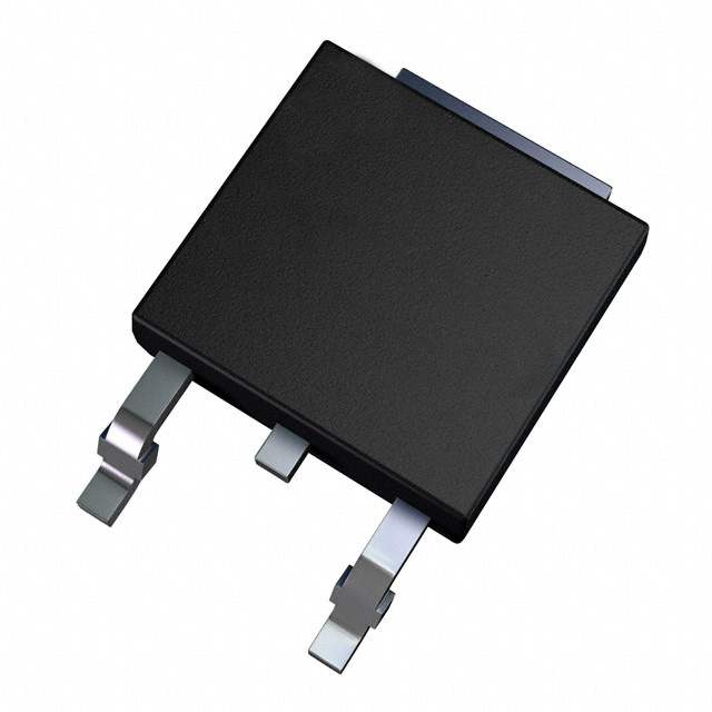
The FQD6N40CTM is an N-Channel MOSFET manufactured by onsemi, rated for 400V drain-to-source voltage with 4.5A continuous drain current at 25°C. This device is housed in a Surface Mount TO-252-3 DPAK package and is part of the QFET® series. The component is Active in product status and fully compliant with RoHS3 and REACH regulations.
Substitute parts are identified when equivalent electrical performance can be achieved within the specified parameter tolerances while maintaining the same package form factor and thermal characteristics. Alternative models may be required due to inventory constraints, supply chain considerations, or application-specific thermal management needs.
Substiute Parts
Key Parameters
| Parameter | Value | Unit |
|---|---|---|
| Drain to Source Voltage (Vdss) | 400 | V |
| Continuous Drain Current (Id) @ 25°C | 4.5 | A |
| Drive Voltage (Max Rds On) | 10 | V |
| Rds On (Max) @ Id, Vgs | 1 | Ohm @ 2.25A, 10V |
| Gate Threshold Voltage (Vgs(th)) @ Id | 4 | V @ 250µA |
| Gate Charge (Qg) @ Vgs | 20 | nC @ 10V |
| Input Capacitance (Ciss) @ Vds | 625 | pF @ 25V |
| Power Dissipation (Max) | 2.5 / 48 | W (Ta) / W (Tc) |
| Operating Temperature Range | -55 to 150 | °C (TJ) |
| Package Type | TO-252-3 DPAK | Surface Mount |
| RoHS Status | ROHS3 Compliant | - |
| Moisture Sensitivity Level | 1 (Unlimited) | - |
Substitute Part Grouping Explanation
Substitution eligibility for the FQD6N40CTM is determined by the following critical parameters:
Mandatory Matching Criteria:
- Drain to Source Voltage (Vdss): 400V
- Package Type: TO-252-3 DPAK (Surface Mount)
- FET Type: N-Channel MOSFET
- Operating Temperature Range: -55°C to 150°C (TJ)
- RoHS3 Compliance
- Moisture Sensitivity Level: 1 (Unlimited)
Performance Parameters (Allowable Variation):
- Continuous Drain Current (Id): Substitute must meet or exceed 4.5A at 25°C
- Rds On (Max): Substitute must not exceed 1Ohm at specified gate voltage
- Gate Threshold Voltage (Vgs(th)): Substitute must fall within ±30V maximum gate voltage specification
- Gate Charge (Qg): Substitute specifications must be compatible with drive circuit requirements
- Input Capacitance (Ciss): Substitute must be compatible with switching frequency and gate drive characteristics
The identified substitute parts STD5NK40ZT4 and STD7NK40ZT4 share the same 400V Vdss rating, DPAK package configuration, and temperature operating range. Both are manufactured by STMicroelectronics and maintain RoHS3 compliance and MSL 1 rating.
Parameter Comparison
| Parameter | FQD6N40CTM (onsemi) | STD5NK40ZT4 (STMicroelectronics) | STD7NK40ZT4 (STMicroelectronics) |
|---|---|---|---|
| Manufacturer | onsemi | STMicroelectronics | STMicroelectronics |
| Drain to Source Voltage (Vdss) | 400V | 400V | 400V |
| Continuous Drain Current (Id) @ 25°C | 4.5A | 3A | 5.4A |
| Drive Voltage (Max Rds On) | 10V | 10V | 10V |
| Rds On (Max) @ Id, Vgs | 1Ohm @ 2.25A, 10V | 1.8Ohm @ 1.5A, 10V | 1Ohm @ 2.7A, 10V |
| Gate Threshold Voltage (Vgs(th)) @ Id | 4V @ 250µA | 4.5V @ 50µA | 4.5V @ 50µA |
| Gate Charge (Qg) @ Vgs | 20nC @ 10V | 17nC @ 10V | 26nC @ 10V |
| Input Capacitance (Ciss) @ Vds | 625pF @ 25V | 305pF @ 25V | 535pF @ 25V |
| Power Dissipation (Max) | 2.5W (Ta), 48W (Tc) | 45W (Tc) | 70W (Tc) |
| Operating Temperature Range | -55°C to 150°C (TJ) | -55°C to 150°C (TJ) | -55°C to 150°C (TJ) |
| Package Type | TO-252-3 DPAK | TO-252-3 DPAK | TO-252-3 DPAK |
| Mounting Type | Surface Mount | Surface Mount | Surface Mount |
| RoHS Status | ROHS3 Compliant | ROHS3 Compliant | ROHS3 Compliant |
| Moisture Sensitivity Level | 1 (Unlimited) | 1 (Unlimited) | 1 (Unlimited) |
| REACH Status | REACH Unaffected | REACH Unaffected | REACH Unaffected |
Engineering Selection Recommendations
FQD6N40CTM (Primary Part): The FQD6N40CTM is the specified component with Active product status. It delivers 4.5A continuous drain current at 25°C with 1Ohm maximum on-resistance at 10V gate drive. This part is suitable for applications requiring balanced current handling and thermal performance within the 48W (Tc) dissipation limit. Full RoHS3 compliance and REACH unaffected status confirm regulatory alignment.
STD7NK40ZT4 (Higher Current Substitute): The STD7NK40ZT4 provides 5.4A continuous drain current, exceeding the FQD6N40CTM specification by 20%. It maintains identical 1Ohm on-resistance at 10V gate drive and offers superior thermal performance at 70W (Tc) maximum dissipation. This substitute is suitable for applications where higher current capacity or improved thermal headroom is beneficial. Gate charge increases to 26nC, requiring verification of gate drive circuit compatibility. Active product status, RoHS3 compliance, and REACH unaffected status are maintained.
STD5NK40ZT4 (Lower Current Substitute): The STD5NK40ZT4 provides 3A continuous drain current, representing a 33% reduction from the FQD6N40CTM specification. On-resistance increases to 1.8Ohm at 10V gate drive. This substitute is suitable only for applications where the lower current rating is acceptable and thermal constraints are less demanding. Gate charge reduces to 17nC, improving gate drive efficiency. Active product status, RoHS3 compliance, and REACH unaffected status are maintained.
All three parts share identical 400V Vdss rating, TO-252-3 DPAK package configuration, -55°C to 150°C operating temperature range, and regulatory compliance status.
Frequently Asked Questions (FAQ)
Q: Can STD7NK40ZT4 directly replace FQD6N40CTM in all applications?
A: STD7NK40ZT4 shares the same 400V Vdss rating, 1Ohm on-resistance at 10V gate drive, and DPAK package. The higher 5.4A current rating and 70W (Tc) thermal dissipation provide additional performance margin. Gate charge increases from 20nC to 26nC, which may require gate drive circuit evaluation for switching frequency compatibility. Both parts maintain identical operating temperature range and regulatory compliance.
Q: Is STD5NK40ZT4 suitable as a substitute for FQD6N40CTM?
A: STD5NK40ZT4 is suitable only for applications where the 3A continuous drain current rating meets circuit requirements. The 1.8Ohm on-resistance at 10V gate drive represents a 80% increase compared to FQD6N40CTM, resulting in higher power dissipation. Both parts share 400V Vdss, DPAK package, and identical operating temperature range. Thermal analysis is required to confirm acceptability in the target application.
Q: Are all three parts pin-compatible?
A: Yes. FQD6N40CTM, STD5NK40ZT4, and STD7NK40ZT4 all use the TO-252-3 DPAK package with identical pin configuration (2 Leads + Tab). Surface mount placement and soldering procedures are interchangeable.
Q: What is the impact of different gate charge specifications?
A: Gate charge (Qg) varies across the three parts: FQD6N40CTM at 20nC, STD5NK40ZT4 at 17nC, and STD7NK40ZT4 at 26nC. Gate charge affects gate drive circuit current requirements and switching speed. Higher gate charge (STD7NK40ZT4) requires greater gate drive current; lower gate charge (STD5NK40ZT4) reduces gate drive requirements. Gate drive circuit design must accommodate the selected part's gate charge specification.
Q: Do all substitute parts maintain the same regulatory compliance?
A: Yes. FQD6N40CTM, STD5NK40ZT4, and STD7NK40ZT4 are all RoHS3 compliant, REACH unaffected, and carry MSL 1 (Unlimited) moisture sensitivity rating. All parts are Active in product status.
Q: What are the input capacitance differences, and do they matter?
A: Input capacitance (Ciss) values are FQD6N40CTM at 625pF, STD5NK40ZT4 at 305pF, and STD7NK40ZT4 at 535pF. Input capacitance affects gate drive circuit impedance and switching transient behavior. Lower capacitance (STD5NK40ZT4) reduces gate drive loading; higher capacitance (FQD6N40CTM) increases gate drive requirements. Selection depends on gate drive circuit design and switching frequency specifications.
Q: Can these parts be used interchangeably in high-frequency switching applications?
A: Interchangeability in high-frequency applications depends on gate charge and input capacitance compatibility with the gate drive circuit. STD7NK40ZT4 has higher gate charge (26nC) and input capacitance (535pF), requiring higher gate drive current. STD5NK40ZT4 has lower values (17nC and 305pF), reducing gate drive requirements. Gate drive circuit design must be evaluated for each part selection.
Alternative Parts

SJ6012L2TP
Littelfuse Inc.
6 Alternative Parts

JMK107BBJ476MA-RE
Taiyo Yuden
10 Alternative Parts

GMK107BBJ475MA-T
Taiyo Yuden
5 Alternative Parts
SJ6020N2ARP
Littelfuse Inc.
3 Alternative Parts
SJ6025R2ATP
Littelfuse Inc.
4 Alternative Parts

2474-05L
API Delevan Inc.
1 Alternative Parts

4590R-684K
API Delevan Inc.
1 Alternative Parts

CM6560R-334
API Delevan Inc.
1 Alternative Parts

CM6460-104
API Delevan Inc.
1 Alternative Parts

5526-12
API Delevan Inc.
1 Alternative Parts