


Request Quote
(Ships tomorrow)
FQD630TM Equivalent & Substitute Parts
Part Overview
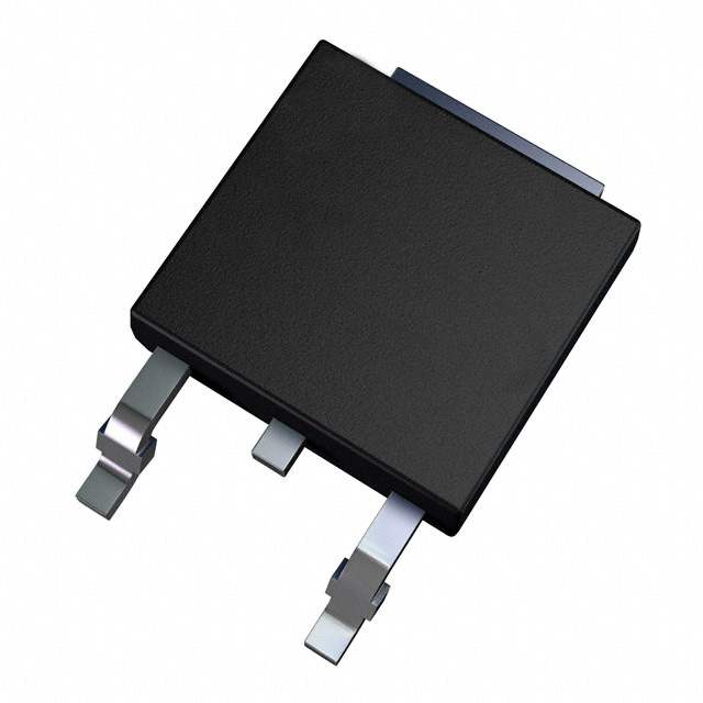
The FQD630TM is an N-Channel MOSFET manufactured by onsemi, rated for 200V drain-to-source voltage with 7A continuous drain current at 25°C (Tc). This device is housed in a TO-252AA (DPAK) surface mount package and is classified as obsolete. The FQD630TM operates across a temperature range of -55°C to 150°C and is part of the QFET® series.
Due to the obsolete product status of the FQD630TM, identifying equivalent substitute parts is necessary to maintain design continuity and ensure component availability for new production runs and field replacements. Substitute parts must maintain electrical and mechanical compatibility within the specified parameter tolerances.
Substiute Parts
Key Parameters
| Parameter | FQD630TM Value | Unit |
|---|---|---|
| Drain-to-Source Voltage (Vdss) | 200 | V |
| Continuous Drain Current (Id) @ 25°C | 7 | A (Tc) |
| Rds On (Max) @ Id, Vgs | 400 mOhm @ 3.5A, 10V | mOhm |
| Gate Threshold Voltage (Vgs(th)) (Max) @ Id | 4 | V @ 250µA |
| Gate Charge (Qg) (Max) @ Vgs | 25 | nC @ 10V |
| Maximum Gate Voltage (Vgs) | ±25 | V |
| Input Capacitance (Ciss) (Max) @ Vds | 550 | pF @ 25V |
| Power Dissipation (Max) | 2.5 (Ta), 46 (Tc) | W |
| Operating Temperature Range | -55 to 150 | °C (TJ) |
| Package Type | TO-252-3, DPAK | Surface Mount |
| Moisture Sensitivity Level (MSL) | 1 (Unlimited) | - |
Substitute Part Grouping Explanation
Substitute parts for the FQD630TM are identified based on strict electrical and mechanical parameter alignment. The following criteria determine substitution eligibility:
Critical Matching Parameters:
- Drain-to-Source Voltage (Vdss): Must equal or exceed 200V
- Package Type: Must be TO-252 (DPAK) surface mount configuration
- FET Type: Must be N-Channel MOSFET technology
- Rds On (Max): Must not exceed 400 mOhm at specified gate and drain conditions
- Operating Temperature Range: Must support minimum -55°C to 150°C operation
- Moisture Sensitivity Level: Must be MSL 1 or equivalent
The AOD4504 meets these substitution criteria through equivalent voltage rating, matching package configuration, comparable on-resistance characteristics, and compatible temperature operating range. Both devices share identical Vdss (200V), matching Rds On specifications (400 mOhm @ 10V), and identical MSL classification.
Parameter Comparison
| Parameter | FQD630TM | AOD4504 | Unit |
|---|---|---|---|
| Manufacturer | onsemi | Alpha & Omega Semiconductor Inc. | - |
| Product Status | Obsolete | Active | - |
| FET Type | N-Channel | N-Channel | - |
| Drain-to-Source Voltage (Vdss) | 200 | 200 | V |
| Continuous Drain Current (Id) @ 25°C | 7 (Tc) | 6 (Tc) | A |
| Rds On (Max) @ Id, Vgs | 400 @ 3.5A, 10V | 400 @ 3A, 10V | mOhm |
| Gate Threshold Voltage (Vgs(th)) (Max) @ Id | 4 @ 250µA | 3.7 @ 250µA | V |
| Gate Charge (Qg) (Max) @ Vgs | 25 @ 10V | 115 @ 10V | nC |
| Maximum Gate Voltage (Vgs) | ±25 | ±20 | V |
| Input Capacitance (Ciss) (Max) @ Vds | 550 @ 25V | 328 @ 100V | pF |
| Power Dissipation (Max) | 2.5 (Ta), 46 (Tc) | 2.5 (Ta), 42.5 (Tc) | W |
| Operating Temperature Range | -55 to 150 | -55 to 175 | °C (TJ) |
| Package Type | TO-252-3, DPAK | TO-252-3, DPAK | Surface Mount |
| Moisture Sensitivity Level (MSL) | 1 (Unlimited) | 1 (Unlimited) | - |
| REACH Status | REACH Unaffected | REACH Unaffected | - |
| ECCN | EAR99 | EAR99 | - |
Engineering Selection Recommendations
AOD4504 as Primary Substitute:
The AOD4504 is the qualified substitute for the obsolete FQD630TM based on the following engineering criteria:
-
Electrical Compatibility: Both devices share identical Vdss (200V) and matching Rds On specifications (400 mOhm @ 10V). The AOD4504 continuous drain current of 6A (Tc) is within acceptable tolerance of the FQD630TM's 7A (Tc) rating for most applications operating below maximum current conditions.
-
Package Compatibility: Both devices utilize the TO-252-3 DPAK surface mount package, enabling direct PCB footprint compatibility without layout modifications.
-
Product Status: The AOD4504 maintains active product status with 20,300 pieces in stock, ensuring long-term availability compared to the obsolete FQD630TM.
-
Regulatory Compliance: Both devices carry identical REACH Unaffected and EAR99 ECCN classifications, maintaining compliance requirements across supply chains.
-
Temperature Performance: The AOD4504 extends the maximum operating temperature to 175°C (versus 150°C for FQD630TM), providing enhanced thermal margin in high-temperature applications.
-
RoHS Compliance: The AOD4504 is ROHS3 compliant, meeting current environmental standards for new production designs.
Design Considerations:
The AOD4504 exhibits higher gate charge (115 nC versus 25 nC) and lower maximum gate voltage (±20V versus ±25V). Applications utilizing gate drive circuits must accommodate these parameter differences. The reduced input capacitance of the AOD4504 (328 pF @ 100V versus 550 pF @ 25V) may improve switching performance in high-frequency applications.
Frequently Asked Questions (FAQ)
Q: Can the AOD4504 directly replace the FQD630TM without PCB modifications?
A: Yes. Both devices use identical TO-252-3 DPAK surface mount packages with matching pin configurations and footprints. No PCB layout changes are required for mechanical substitution.
Q: What is the significance of the continuous drain current difference (7A versus 6A)?
A: The AOD4504's 6A (Tc) rating is approximately 86% of the FQD630TM's 7A (Tc) specification. Applications operating continuously at or above 6.5A require thermal analysis to confirm the AOD4504 remains within acceptable junction temperature limits. Applications operating below 6A experience no current-related limitations.
Q: How do the gate charge differences affect circuit design?
A: The AOD4504's gate charge of 115 nC (versus 25 nC for FQD630TM) requires proportionally longer switching times with identical gate drive current. Gate drive circuits must supply sufficient current to achieve required switching frequencies. Higher gate charge increases power dissipation in the gate drive circuit.
Q: Are there temperature operating range implications?
A: The AOD4504 supports -55°C to 175°C operation, extending 25°C beyond the FQD630TM's -55°C to 150°C range. This provides additional thermal margin for high-temperature applications. Both devices maintain identical minimum temperature specifications.
Q: What compliance certifications apply to the AOD4504?
A: The AOD4504 carries ROHS3 compliance, REACH Unaffected status, and EAR99 ECCN classification. These certifications match the FQD630TM's regulatory profile, ensuring equivalent compliance for supply chain and export requirements.
Q: Does the lower maximum gate voltage (±20V versus ±25V) create compatibility issues?
A: Applications using gate drive voltages at or below ±20V experience no limitations. Designs utilizing ±25V gate drive signals must be evaluated to confirm operation within the AOD4504's ±20V specification. Most standard gate drive circuits operate within ±15V, making this difference non-critical for typical applications.
Q: How does the input capacitance difference impact high-frequency performance?
A: The AOD4504's lower input capacitance (328 pF @ 100V versus 550 pF @ 25V) reduces capacitive loading on gate drive circuits, potentially improving switching speed and reducing gate drive power dissipation in high-frequency applications above 100 kHz.
Alternative Parts

SJ6012L2TP
Littelfuse Inc.
6 Alternative Parts

JMK107BBJ476MA-RE
Taiyo Yuden
10 Alternative Parts

GMK107BBJ475MA-T
Taiyo Yuden
5 Alternative Parts
SJ6020N2ARP
Littelfuse Inc.
3 Alternative Parts
SJ6025R2ATP
Littelfuse Inc.
4 Alternative Parts

2474-05L
API Delevan Inc.
1 Alternative Parts

4590R-684K
API Delevan Inc.
1 Alternative Parts

CM6560R-334
API Delevan Inc.
1 Alternative Parts

CM6460-104
API Delevan Inc.
1 Alternative Parts

5526-12
API Delevan Inc.
1 Alternative Parts