


Request Quote
(Ships tomorrow)
FJMA790 Equivalent & Substitute Parts
Part Overview
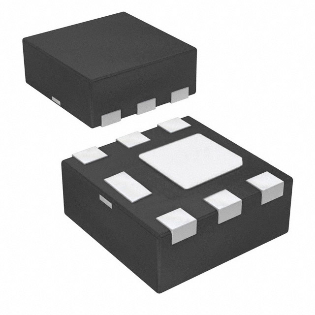
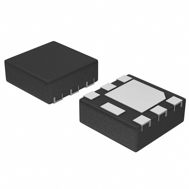
The FJMA790 is a PNP bipolar junction transistor manufactured by onsemi, rated for 35 V collector-emitter breakdown voltage and 2 A maximum collector current. The device is packaged in a 6-MicroFET (2x2) surface mount configuration with a maximum power dissipation of 1.56 W. The FJMA790 is classified as obsolete, making equivalent and substitute parts necessary for ongoing design support and procurement continuity. Substitute parts must maintain electrical compatibility across critical parameters including collector current rating, voltage rating, and saturation characteristics while accommodating potential package and performance variations.
Substiute Parts
Key Parameters
| Parameter | FJMA790 Specification |
|---|---|
| Transistor Type | PNP |
| Current - Collector (Ic) (Max) | 2 A |
| Voltage - Collector Emitter Breakdown (Max) | 35 V |
| Vce Saturation (Max) @ Ib, Ic | 450mV @ 50mA, 2A |
| Current - Collector Cutoff (Max) | 100nA (ICBO) |
| DC Current Gain (hFE) (Min) @ Ic, Vce | 100 @ 1.5A, 1.5V |
| Power - Max | 1.56 W |
| Mounting Type | Surface Mount |
| Package / Case | 6-WDFN Exposed Pad |
| Operating Temperature (TJ) | 150°C |
| Product Status | Obsolete |
Substitute Part Grouping Explanation
Substitute parts for the FJMA790 are qualified based on the following electrical and mechanical parameters:
Primary Compatibility Criteria:
- Transistor type: PNP configuration
- Collector current rating: 2 A maximum
- Collector-emitter breakdown voltage: minimum 35 V
- Surface mount packaging with compatible footprint
- Saturation voltage characteristics suitable for switching applications
Substitution Logic:
The NSS35200CF8T1G (Sanyo) maintains the exact 35 V and 2 A ratings as the FJMA790, with improved saturation voltage performance (300mV vs. 450mV) and active product status. However, the package differs (8-SMD ChipFET™ vs. 6-WDFN), requiring PCB layout modification.
The NSS40200UW6T1G and NSV40200UW6T1G (both onsemi) provide higher voltage rating (40 V vs. 35 V) and identical 2 A collector current, with the same 6-WDFN package footprint as the FJMA790. These parts offer superior frequency response (140MHz transition frequency) and improved saturation characteristics. The NSV40200UW6T1G is active product status with tape and reel packaging, while NSS40200UW6T1G is obsolete.
Parameter Comparison
| Parameter | FJMA790 | NSS35200CF8T1G | NSS40200UW6T1G | NSV40200UW6T1G |
|---|---|---|---|---|
| Manufacturer | onsemi | Sanyo | onsemi | onsemi |
| Transistor Type | PNP | PNP | PNP | PNP |
| Current - Collector (Ic) (Max) | 2 A | 2 A | 2 A | 2 A |
| Voltage - Collector Emitter Breakdown (Max) | 35 V | 35 V | 40 V | 40 V |
| Vce Saturation (Max) @ Ib, Ic | 450mV @ 50mA, 2A | 300mV @ 20mA, 2A | 300mV @ 20mA, 2A | 300mV @ 20mA, 2A |
| Current - Collector Cutoff (Max) | 100nA | 100nA | 100nA | 100nA |
| DC Current Gain (hFE) (Min) @ Ic, Vce | 100 @ 1.5A, 1.5V | 100 @ 1.5A, 2V | 150 @ 1A, 2V | 150 @ 1A, 2V |
| Power - Max | 1.56 W | 635 mW | 875 mW | 875 mW |
| Frequency - Transition | Not specified | 100MHz | 140MHz | 140MHz |
| Operating Temperature (TJ) | 150°C | -55°C ~ 150°C | -55°C ~ 150°C | -55°C ~ 150°C |
| Mounting Type | Surface Mount | Surface Mount | Surface Mount | Surface Mount |
| Package / Case | 6-WDFN Exposed Pad | 8-SMD, Flat Lead | 6-WDFN Exposed Pad | 6-WDFN Exposed Pad |
| Product Status | Obsolete | Active | Obsolete | Active |
| RoHS Status | Not specified | Not specified | ROHS3 Compliant | ROHS3 Compliant |
| Moisture Sensitivity Level (MSL) | 1 (Unlimited) | Not specified | 1 (Unlimited) | 1 (Unlimited) |
| REACH Status | REACH Unaffected | Not specified | REACH Unaffected | REACH Unaffected |
Engineering Selection Recommendations
NSV40200UW6T1G (Recommended Primary Substitute)
The NSV40200UW6T1G is the preferred substitute for the FJMA790 based on active product status and full compliance alignment. This onsemi device maintains the identical 6-WDFN package footprint, eliminating PCB redesign requirements. The 40 V voltage rating provides 5 V margin above the FJMA790 specification, enhancing circuit reliability. Improved saturation voltage (300mV vs. 450mV) reduces power dissipation in switching applications. The device is ROHS3 compliant, REACH unaffected, and available in tape and reel packaging for production environments. Moisture sensitivity level 1 matches the original part specification.
NSS40200UW6T1G (Secondary Substitute)
The NSS40200UW6T1G provides identical electrical and package specifications to the NSV40200UW6T1G but carries obsolete product status. This part is suitable for legacy system support or applications where active product status is not a procurement requirement. Electrical performance and compliance certifications are equivalent to the recommended primary substitute.
NSS35200CF8T1G (Alternative Substitute)
The NSS35200CF8T1G maintains the exact 35 V and 2 A ratings of the FJMA790 with active product status from Sanyo. This part offers improved saturation voltage performance and extended operating temperature range (-55°C to 150°C). However, the 8-SMD ChipFET™ package differs from the 6-WDFN footprint, requiring PCB layout modification and design validation. This substitute is appropriate for applications where package compatibility is not constrained and design flexibility exists.
Frequently Asked Questions (FAQ)
Q: Can the NSV40200UW6T1G directly replace the FJMA790 without PCB modifications?
A: Yes. The NSV40200UW6T1G uses the identical 6-WDFN exposed pad package as the FJMA790, enabling direct footprint compatibility. No PCB layout changes are required for mechanical and electrical integration.
Q: What is the significance of the 40 V rating on the NSV40200UW6T1G compared to the FJMA790's 35 V rating?
A: The higher voltage rating provides additional design margin and circuit protection. The NSV40200UW6T1G can operate safely in applications rated up to 40 V, while the FJMA790 is limited to 35 V. This does not create incompatibility; the substitute is suitable for any circuit designed for the original 35 V specification.
Q: Why does the NSS35200CF8T1G have lower maximum power dissipation (635 mW vs. 1.56 W)?
A: The NSS35200CF8T1G uses a different package technology (8-SMD ChipFET™) with different thermal characteristics compared to the 6-WDFN package. The lower power rating reflects the thermal limitations of the ChipFET™ package, not reduced electrical capability. For applications requiring the full 1.56 W dissipation, the 6-WDFN packaged alternatives (NSV40200UW6T1G or NSS40200UW6T1G) are appropriate.
Q: Is the NSS35200CF8T1G suitable for high-frequency applications?
A: The NSS35200CF8T1G specifies 100 MHz transition frequency, compared to 140 MHz for the NSV40200UW6T1G and NSS40200UW6T1G. For applications operating below 100 MHz, the NSS35200CF8T1G is suitable. For higher frequency requirements, the 140 MHz alternatives are recommended.
Q: What packaging format should be selected for production assembly?
A: The NSV40200UW6T1G is available in tape and reel (TR) packaging, suitable for automated pick-and-place assembly. The NSS40200UW6T1G is available in bulk packaging. For high-volume production, tape and reel format reduces handling and improves assembly efficiency.
Q: Are all substitute parts ROHS3 compliant?
A: The NSV40200UW6T1G and NSS40200UW6T1G are explicitly ROHS3 compliant. The NSS35200CF8T1G RoHS status is not specified in the provided data. For applications requiring ROHS3 compliance certification, the onsemi alternatives are confirmed compliant.
Q: What is the moisture sensitivity level for all parts?
A: The FJMA790, NSV40200UW6T1G, and NSS40200UW6T1G all specify MSL 1 (Unlimited), indicating no moisture sensitivity restrictions. The NSS35200CF8T1G MSL rating is not specified in the provided data.
Alternative Parts

SJ6012L2TP
Littelfuse Inc.
6 Alternative Parts

JMK107BBJ476MA-RE
Taiyo Yuden
10 Alternative Parts

GMK107BBJ475MA-T
Taiyo Yuden
5 Alternative Parts
SJ6020N2ARP
Littelfuse Inc.
3 Alternative Parts
SJ6025R2ATP
Littelfuse Inc.
4 Alternative Parts

2474-05L
API Delevan Inc.
1 Alternative Parts

4590R-684K
API Delevan Inc.
1 Alternative Parts

CM6560R-334
API Delevan Inc.
1 Alternative Parts

CM6460-104
API Delevan Inc.
1 Alternative Parts

5526-12
API Delevan Inc.
1 Alternative Parts