


Request Quote
(Ships tomorrow)
FDWS5360L-F085 Equivalent & Substitute Parts
Part Overview
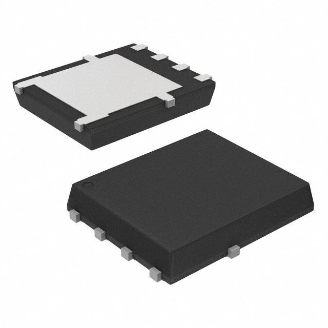
The FDWS5360L-F085 is an N-Channel 60V 60A Power MOSFET manufactured by onsemi in the PowerTrench® series. This device is designed for surface mount applications requiring high current switching capability with a maximum power dissipation of 150W. The part is classified as Obsolete, necessitating identification of functionally equivalent alternatives for ongoing design requirements and production continuity. Substitute parts must maintain electrical compatibility across voltage ratings, current handling, and thermal characteristics while accommodating different package configurations.
Substiute Parts
Key Parameters
| Parameter | Value | Unit |
|---|---|---|
| Drain to Source Voltage (Vdss) | 60 | V |
| Continuous Drain Current (Id) @ 25°C | 60 | A |
| On-State Resistance (Rds On Max) @ 60A, 10V | 8.5 | mOhm |
| Gate Threshold Voltage (Vgs(th) Max) @ 250µA | 3 | V |
| Gate Charge (Qg Max) @ 10V | 72 | nC |
| Power Dissipation (Max) | 150 | W |
| Operating Temperature Range | -55 to 175 | °C |
| Package Type | 8-PowerVDFN | — |
| Qualification Standard | AEC-Q101 | — |
Substitute Part Grouping Explanation
Substitution of the FDWS5360L-F085 is determined by the following critical electrical and mechanical parameters:
Voltage Rating Compatibility: The substitute part must maintain a Drain to Source Voltage (Vdss) rating of 60V or greater to ensure safe operation across all specified application conditions.
Current Handling: The substitute part must support continuous drain current (Id) at or above the application requirement. The FDWS5360L-F085 operates at 60A; substitute parts with lower current ratings (such as 50A) are acceptable only when application current demands do not exceed the substitute's rating.
On-State Resistance (Rds On): The substitute must demonstrate Rds On characteristics compatible with thermal and efficiency requirements. Variations in Rds On directly affect power dissipation and heat generation.
Gate Charge and Threshold Voltage: These parameters affect switching speed and drive circuit requirements. Substitutes must operate within the same gate drive voltage range (4.5V to 10V) to maintain compatibility with existing driver circuits.
Temperature Range: The substitute must support the full operating temperature range of -55°C to 175°C (Tj).
Qualification and Compliance: Both the main part and substitute must carry AEC-Q101 automotive qualification to maintain design integrity in regulated applications.
Package Configuration: While the main part uses 8-PowerVDFN packaging, substitute parts may employ different surface mount packages (such as 5-DFN) provided the physical footprint and thermal characteristics are evaluated for the specific application.
Parameter Comparison
| Parameter | FDWS5360L-F085 | NVMFS5C673NLWFAFT1G | Unit |
|---|---|---|---|
| Manufacturer | onsemi | onsemi | — |
| FET Type | N-Channel | N-Channel | — |
| Technology | MOSFET (Metal Oxide) | MOSFET (Metal Oxide) | — |
| Drain to Source Voltage (Vdss) | 60 | 60 | V |
| Continuous Drain Current (Id) @ 25°C | 60 | 50 | A |
| Drive Voltage (Max Rds On, Min Rds On) | 4.5V, 10V | 4.5V, 10V | — |
| Rds On (Max) @ Vgs 10V | 8.5 @ 60A | 9.2 @ 25A | mOhm |
| Gate Threshold Voltage (Vgs(th) Max) | 3 @ 250µA | 2 @ 35µA | V |
| Gate Charge (Qg Max) @ 10V | 72 | 9.5 | nC |
| Vgs (Max) | ±20 | ±20 | V |
| Input Capacitance (Ciss Max) | 3695 @ 30V | 880 @ 25V | pF |
| Power Dissipation (Max) | 150 | 46 | W |
| Operating Temperature Range | -55 to 175 | -55 to 175 | °C |
| Grade | Automotive | Automotive | — |
| Qualification | AEC-Q101 | AEC-Q101 | — |
| Mounting Type | Surface Mount | Surface Mount | — |
| Package / Case | 8-PowerVDFN | 8-PowerTDFN, 5 Leads | — |
| Product Status | Obsolete | Active | — |
| Moisture Sensitivity Level (MSL) | 1 (Unlimited) | 1 (Unlimited) | — |
| REACH Status | REACH Unaffected | REACH Unaffected | — |
| ECCN | EAR99 | EAR99 | — |
Engineering Selection Recommendations
Product Status Consideration: The FDWS5360L-F085 is classified as Obsolete. The NVMFS5C673NLWFAFT1G is classified as Active, ensuring long-term availability and continued manufacturing support.
Electrical Compatibility: Both parts share identical voltage ratings (60V Vdss) and gate drive voltage requirements (4.5V to 10V). Both maintain AEC-Q101 automotive qualification and operate across the full temperature range of -55°C to 175°C.
Current Rating Differential: The NVMFS5C673NLWFAFT1G is rated for 50A continuous drain current compared to the FDWS5360L-F085 at 60A. This 10A reduction requires evaluation against actual application current demands. Applications operating at or below 50A continuous current are electrically compatible.
Power Dissipation: The NVMFS5C673NLWFAFT1G has a maximum power dissipation of 46W compared to 150W for the FDWS5360L-F085. This reflects the lower current rating and different package thermal characteristics. Thermal analysis of the specific application is necessary to confirm adequate heat dissipation with the substitute part.
Gate Charge Reduction: The NVMFS5C673NLWFAFT1G exhibits significantly lower gate charge (9.5 nC versus 72 nC), resulting in faster switching characteristics and reduced driver circuit stress.
Package Transition: The NVMFS5C673NLWFAFT1G uses 8-PowerTDFN packaging with 5 leads, differing from the 8-PowerVDFN package of the main part. PCB layout and thermal management design must be re-evaluated for the new package footprint.
Compliance Alignment: Both parts maintain REACH Unaffected status and EAR99 export classification, ensuring regulatory continuity.
Frequently Asked Questions (FAQ)
Q: Can the NVMFS5C673NLWFAFT1G directly replace the FDWS5360L-F085 in all applications?
A: Direct replacement is limited by current rating. The NVMFS5C673NLWFAFT1G is rated for 50A continuous drain current versus 60A for the FDWS5360L-F085. Applications requiring continuous current above 50A are not compatible. Additionally, the package change from 8-PowerVDFN to 8-PowerTDFN requires PCB layout modification.
Q: What is the significance of the lower gate charge in the NVMFS5C673NLWFAFT1G?
A: Lower gate charge (9.5 nC versus 72 nC) reduces the charge that must be supplied by the gate driver circuit, resulting in faster switching transitions and lower driver power consumption. Existing gate driver circuits designed for the FDWS5360L-F085 will operate with improved performance characteristics.
Q: Are both parts qualified for automotive applications?
A: Yes. Both the FDWS5360L-F085 and NVMFS5C673NLWFAFT1G carry AEC-Q101 automotive qualification and are classified as Automotive grade, meeting automotive reliability and quality standards.
Q: How does the power dissipation difference affect thermal design?
A: The NVMFS5C673NLWFAFT1G has a maximum power dissipation rating of 46W compared to 150W for the FDWS5360L-F085. This reflects the lower current rating and different package thermal resistance. Thermal analysis specific to the application environment and PCB design is required to confirm adequate heat dissipation.
Q: What packaging considerations apply to the NVMFS5C673NLWFAFT1G?
A: The NVMFS5C673NLWFAFT1G uses 8-PowerTDFN packaging with 5 leads, whereas the FDWS5360L-F085 uses 8-PowerVDFN. The different package footprint requires PCB redesign. Thermal vias and copper area allocation must be re-evaluated for the new package geometry.
Q: Are the gate drive voltage requirements identical between the two parts?
A: Yes. Both parts specify drive voltage ranges of 4.5V (Max Rds On) and 10V (Min Rds On), with maximum gate voltage ratings of ±20V. Existing gate driver circuits designed for the FDWS5360L-F085 are electrically compatible with the NVMFS5C673NLWFAFT1G.
Q: What is the operating temperature range for both parts?
A: Both the FDWS5360L-F085 and NVMFS5C673NLWFAFT1G operate across the full temperature range of -55°C to 175°C (Tj), ensuring compatibility across automotive environmental specifications.
Q: Why is the FDWS5360L-F085 classified as Obsolete?
A: Obsolete status indicates that the manufacturer has discontinued production and support for this part. The NVMFS5C673NLWFAFT1G, classified as Active, represents the current manufacturing alternative with ongoing availability and support.
Alternative Parts

SJ6012L2TP
Littelfuse Inc.
6 Alternative Parts

JMK107BBJ476MA-RE
Taiyo Yuden
10 Alternative Parts

GMK107BBJ475MA-T
Taiyo Yuden
5 Alternative Parts
SJ6020N2ARP
Littelfuse Inc.
3 Alternative Parts
SJ6025R2ATP
Littelfuse Inc.
4 Alternative Parts

2474-05L
API Delevan Inc.
1 Alternative Parts

4590R-684K
API Delevan Inc.
1 Alternative Parts

CM6560R-334
API Delevan Inc.
1 Alternative Parts

CM6460-104
API Delevan Inc.
1 Alternative Parts

5526-12
API Delevan Inc.
1 Alternative Parts