


Request Quote
(Ships tomorrow)
FDW2508P Equivalent & Substitute Parts
Part Overview
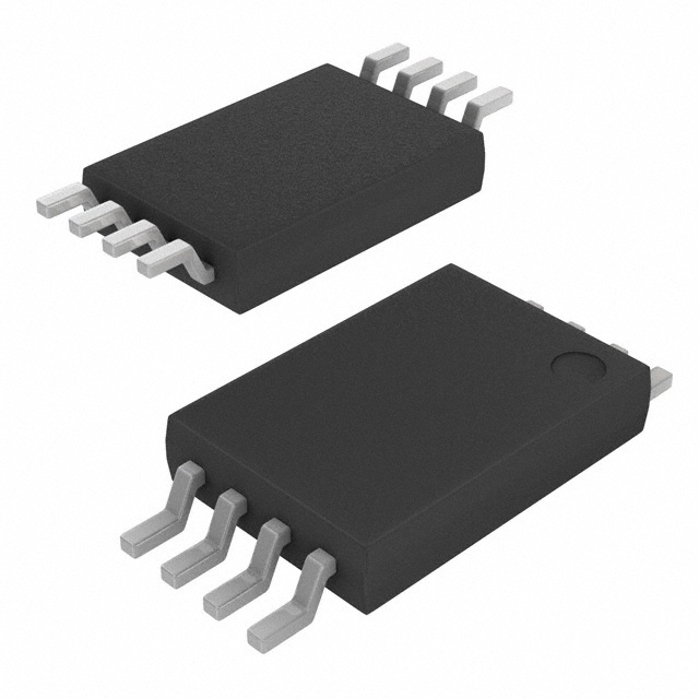
The FDW2508P is a dual P-channel MOSFET array manufactured by onsemi, designed for surface mount applications in the PowerTrench® series. This device integrates two P-channel MOSFETs in a single 8-TSSOP package, rated for 12V drain-to-source voltage and 6A continuous drain current at 25°C. The FDW2508P is classified as obsolete, necessitating identification of active equivalent and substitute components for new designs and ongoing production requirements. Substitute parts must maintain functional compatibility while accounting for differences in electrical ratings and package configurations.
Substiute Parts
Key Parameters
| Parameter | FDW2508P |
|---|---|
| Manufacturer | onsemi |
| Configuration | 2 P-Channel (Dual) |
| Drain to Source Voltage (Vdss) | 12V |
| Current - Continuous Drain (Id) @ 25°C | 6A |
| Rds On (Max) @ Id, Vgs | 18mOhm @ 6A, 4.5V |
| Vgs(th) (Max) @ Id | 1.5V @ 250µA |
| Gate Charge (Qg) (Max) @ Vgs | 36nC @ 4.5V |
| Input Capacitance (Ciss) (Max) @ Vds | 2644pF @ 6V |
| Power - Max | 1W |
| Operating Temperature Range | -55°C ~ 150°C (TJ) |
| Package / Case | 8-TSSOP (0.173", 4.40mm Width) |
| Product Status | Obsolete |
| Moisture Sensitivity Level (MSL) | 1 (Unlimited) |
Substitute Part Grouping Explanation
Substitution of the FDW2508P is determined by the following critical parameters:
Configuration Match: Both the main part and substitute must feature a dual P-channel MOSFET configuration to maintain circuit functionality.
Voltage Rating Compatibility: The substitute part must have a Vdss rating equal to or greater than the original 12V specification. The NTMD6P02R2G provides 20V, which exceeds the minimum requirement and ensures compatibility in applications operating at or below 12V.
Current Handling Capability: The substitute must support the required continuous drain current. The FDW2508P specifies 6A at 25°C, while the NTMD6P02R2G provides 4.8A. This represents a reduction in current capacity and requires circuit-level evaluation for applications demanding the full 6A specification.
On-Resistance (Rds On): The FDW2508P specifies 18mOhm at 6A and 4.5V gate-source voltage. The NTMD6P02R2G specifies 33mOhm at 6.2A and 4.5V gate-source voltage. The higher on-resistance of the substitute results in increased power dissipation and heat generation.
Gate Threshold Voltage (Vgs(th)): Both parts maintain logic-level gate operation with threshold voltages suitable for standard digital control circuits.
Thermal Operating Range: Both parts operate across the identical temperature range of -55°C to 150°C junction temperature, ensuring thermal compatibility.
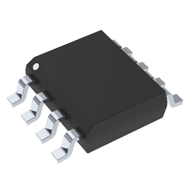
Package Consideration: The FDW2508P uses 8-TSSOP packaging while the NTMD6P02R2G uses 8-SOIC packaging. Both are surface mount configurations with different physical footprints, requiring PCB layout modification.
Parameter Comparison
| Parameter | FDW2508P | NTMD6P02R2G | Notes |
|---|---|---|---|
| Manufacturer | onsemi | onsemi | Same manufacturer |
| Configuration | 2 P-Channel (Dual) | 2 P-Channel (Dual) | Identical configuration |
| Technology | MOSFET (Metal Oxide) | MOSFET (Metal Oxide) | Same technology |
| FET Feature | Logic Level Gate | Logic Level Gate | Identical gate operation |
| Drain to Source Voltage (Vdss) | 12V | 20V | Substitute rated higher |
| Current - Continuous Drain (Id) @ 25°C | 6A | 4.8A | Substitute rated lower |
| Rds On (Max) @ Id, Vgs | 18mOhm @ 6A, 4.5V | 33mOhm @ 6.2A, 4.5V | Substitute has higher resistance |
| Vgs(th) (Max) @ Id | 1.5V @ 250µA | 1.2V @ 250µA | Substitute has lower threshold |
| Gate Charge (Qg) (Max) @ Vgs | 36nC @ 4.5V | 35nC @ 4.5V | Comparable gate charge |
| Input Capacitance (Ciss) (Max) @ Vds | 2644pF @ 6V | 1700pF @ 16V | Substitute has lower capacitance |
| Power - Max | 1W | 750mW | Substitute rated lower |
| Operating Temperature Range | -55°C ~ 150°C (TJ) | -55°C ~ 150°C (TJ) | Identical range |
| Mounting Type | Surface Mount | Surface Mount | Same mounting type |
| Package / Case | 8-TSSOP (0.173", 4.40mm Width) | 8-SOIC (0.154", 3.90mm Width) | Different package footprints |
| Product Status | Obsolete | Active | Substitute is in active production |
| Moisture Sensitivity Level (MSL) | 1 (Unlimited) | 1 (Unlimited) | Identical MSL rating |
| REACH Status | REACH Unaffected | REACH Unaffected | Same compliance status |
Engineering Selection Recommendations
The NTMD6P02R2G is identified as an active substitute for the obsolete FDW2508P based on the following engineering criteria:
Product Status Alignment: The FDW2508P is classified as obsolete, making continued sourcing problematic for production and design continuation. The NTMD6P02R2G maintains active product status with current manufacturing availability, ensuring long-term supply chain viability.
Regulatory Compliance: Both parts maintain identical REACH compliance status (REACH Unaffected) and identical moisture sensitivity levels (MSL 1 - Unlimited), ensuring no additional handling or environmental requirements are introduced through substitution.
Functional Configuration: Both devices feature dual P-channel MOSFET configurations with logic-level gate operation, maintaining circuit-level compatibility for control and switching applications.
Electrical Rating Considerations: The NTMD6P02R2G provides a higher voltage rating (20V versus 12V), which is compatible with applications designed for 12V operation. However, the reduced continuous drain current (4.8A versus 6A) and increased on-resistance (33mOhm versus 18mOhm) require circuit-level analysis to confirm suitability for applications demanding the full current specification or operating at maximum power dissipation limits.
Package Transition: Substitution requires PCB layout modification due to different package footprints (8-TSSOP versus 8-SOIC). Design teams must update schematic symbols, footprints, and board layouts accordingly.
Frequently Asked Questions (FAQ)
Q: Can the NTMD6P02R2G directly replace the FDW2508P without circuit modification?
A: Direct replacement requires PCB layout changes due to different package footprints (8-TSSOP versus 8-SOIC). Electrical compatibility depends on application current requirements. Applications requiring continuous drain current above 4.8A cannot use the NTMD6P02R2G without circuit redesign.
Q: What is the impact of the higher on-resistance in the NTMD6P02R2G?
A: The NTMD6P02R2G specifies 33mOhm on-resistance compared to 18mOhm for the FDW2508P. This increases power dissipation according to P = I²R. At 4.8A, the NTMD6P02R2G dissipates approximately 0.76W, approaching its 750mW maximum power rating. Thermal management and heat dissipation must be evaluated for the specific application.
Q: Are there any gate drive differences between these parts?
A: Both parts feature logic-level gate operation with comparable gate charge specifications (36nC versus 35nC at 4.5V). Gate drive circuits designed for the FDW2508P are compatible with the NTMD6P02R2G without modification.
Q: What is the significance of the voltage rating difference?
A: The NTMD6P02R2G provides 20V drain-to-source voltage rating compared to 12V for the FDW2508P. This higher rating is compatible with 12V applications and provides additional margin for transient voltage spikes. No circuit modification is required due to the higher voltage rating.
Q: How does the lower input capacitance of the NTMD6P02R2G affect circuit performance?
A: The NTMD6P02R2G specifies 1700pF input capacitance at 16V compared to 2644pF for the FDW2508P at 6V. Lower input capacitance reduces gate drive current requirements and improves switching speed. This generally benefits high-frequency switching applications.
Q: Is the NTMD6P02R2G suitable for all applications currently using the FDW2508P?
A: Suitability depends on specific application requirements. Applications operating at continuous drain currents below 4.8A and power dissipation below 750mW are compatible. Applications requiring the full 6A current specification or operating at maximum power dissipation require alternative solutions or circuit redesign.
Q: What packaging considerations apply to this substitution?
A: The FDW2508P uses 8-TSSOP packaging (0.173" width) while the NTMD6P02R2G uses 8-SOIC packaging (0.154" width). PCB footprints, schematic symbols, and board layouts must be updated. Both are standard surface mount packages with established manufacturing processes.
Alternative Parts

SJ6012L2TP
Littelfuse Inc.
6 Alternative Parts

JMK107BBJ476MA-RE
Taiyo Yuden
10 Alternative Parts

GMK107BBJ475MA-T
Taiyo Yuden
5 Alternative Parts
SJ6020N2ARP
Littelfuse Inc.
3 Alternative Parts
SJ6025R2ATP
Littelfuse Inc.
4 Alternative Parts

2474-05L
API Delevan Inc.
1 Alternative Parts

4590R-684K
API Delevan Inc.
1 Alternative Parts

CM6560R-334
API Delevan Inc.
1 Alternative Parts

CM6460-104
API Delevan Inc.
1 Alternative Parts

5526-12
API Delevan Inc.
1 Alternative Parts