


Request Quote
(Ships tomorrow)
FDU6N25 Equivalent & Substitute Parts
Part Overview
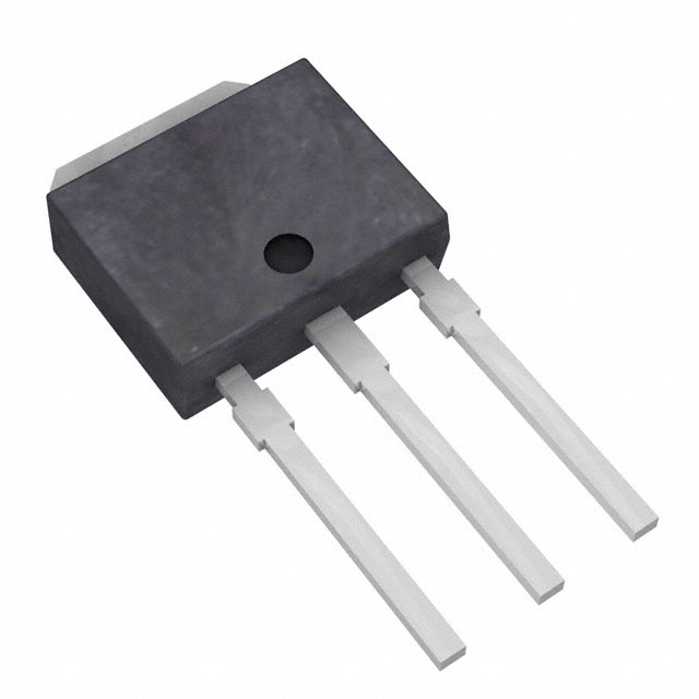
The FDU6N25 is an N-Channel MOSFET manufactured by onsemi, rated for 250V drain-to-source voltage with 4.4A continuous drain current at 25°C. This device features a Through Hole I-PAK (TO-251-3 Stub Leads) package and is designed for 50W power dissipation. The FDU6N25 is classified as Obsolete, making identification of functionally equivalent substitute components necessary for ongoing design support and procurement continuity.
Substiute Parts
Key Parameters
| Parameter | Value | Unit |
|---|---|---|
| Drain to Source Voltage (Vdss) | 250 | V |
| Continuous Drain Current (Id) @ 25°C | 4.4 | A (Tc) |
| Rds On (Max) @ Id, Vgs | 1.1 | Ohm @ 2.2A, 10V |
| Gate Threshold Voltage Vgs(th) (Max) | 5 | V @ 250µA |
| Power Dissipation (Max) | 50 | W (Tc) |
| Operating Temperature Range | -55 to 150 | °C (TJ) |
| Package Type | TO-251-3 Stub Leads, I-PAK | Through Hole |
| Gate Charge (Qg) (Max) @ Vgs | 6 | nC @ 10V |
| Input Capacitance (Ciss) (Max) @ Vds | 250 | pF @ 25V |
Substitute Part Grouping Explanation
Substitution of the FDU6N25 is determined by electrical and mechanical parameter compatibility within the N-Channel MOSFET category. The following parameters establish substitution validity:
Critical Matching Parameters:
- Drain to Source Voltage (Vdss): 250V minimum required
- FET Type: N-Channel topology
- Technology: MOSFET (Metal Oxide)
- Mounting Type: Through Hole
- Package Family: TO-251 variant (I-PAK)
Performance Parameters:
- Continuous Drain Current (Id): Substitute must meet or exceed 4.4A @ 25°C
- On-State Resistance (Rds On): Maximum 1.1 Ohm @ specified gate voltage
- Power Dissipation: Minimum 42W capability
- Operating Temperature Range: -55°C to 150°C
Gate Drive Parameters:
- Gate Threshold Voltage (Vgs(th)): Maximum 5V @ 250µA
- Gate Charge (Qg): Electrical compatibility within switching applications
- Input Capacitance (Ciss): Acceptable range for gate drive circuits
The IRFU224PBF meets these substitution criteria with equivalent voltage rating, compatible package configuration, and electrical performance within acceptable tolerances.
Parameter Comparison
| Parameter | FDU6N25 (Main) | IRFU224PBF (Substitute) | Unit |
|---|---|---|---|
| Manufacturer | onsemi | Vishay Siliconix | - |
| FET Type | N-Channel | N-Channel | - |
| Technology | MOSFET (Metal Oxide) | MOSFET (Metal Oxide) | - |
| Drain to Source Voltage (Vdss) | 250 | 250 | V |
| Continuous Drain Current (Id) @ 25°C | 4.4 | 3.8 | A (Tc) |
| Rds On (Max) @ Id, Vgs | 1.1 @ 2.2A, 10V | 1.1 @ 2.3A, 10V | Ohm |
| Gate Threshold Voltage Vgs(th) (Max) | 5 @ 250µA | 4 @ 250µA | V |
| Gate Charge (Qg) (Max) @ Vgs | 6 @ 10V | 14 @ 10V | nC |
| Vgs (Max) | ±30 | ±20 | V |
| Input Capacitance (Ciss) (Max) @ Vds | 250 @ 25V | 260 @ 25V | pF |
| Power Dissipation (Max) | 50 (Tc) | 42 (Tc) | W |
| Operating Temperature Range | -55 to 150 | -55 to 150 | °C (TJ) |
| Mounting Type | Through Hole | Through Hole | - |
| Package / Case | TO-251-3 Stub Leads, I-PAK | TO-251-3 Short Leads, I-PAK, TO-251AA | - |
| Product Status | Obsolete | Active | - |
| RoHS Status | ROHS3 Compliant | ROHS3 Compliant | - |
Engineering Selection Recommendations
FDU6N25 (Main Part): The FDU6N25 is classified as Obsolete. While 3950 pieces remain in stock, this part number is no longer in active production. New designs should not incorporate this component. Existing applications using the FDU6N25 require transition planning to an active substitute.
IRFU224PBF (Substitute): The IRFU224PBF is an Active product manufactured by Vishay Siliconix with 1210 pieces in stock. This device provides electrical equivalence to the FDU6N25 with the following considerations:
- Voltage Rating: Identical 250V Vdss rating ensures direct voltage compatibility
- Current Rating: 3.8A continuous drain current is 0.6A lower than the FDU6N25 (4.4A). Applications operating below 3.8A experience no derating
- On-State Resistance: Equivalent 1.1 Ohm Rds On at 10V gate voltage maintains switching performance
- Gate Threshold: IRFU224PBF threshold of 4V is lower than FDU6N25 (5V), providing improved gate drive margin
- Power Dissipation: 42W (Tc) rating is 8W lower than FDU6N25 (50W). Thermal design review required for applications approaching 42W dissipation
- Package Configuration: Both devices use TO-251-3 I-PAK Through Hole packages. Lead length differences (Stub vs. Short Leads) require PCB layout verification
- Compliance: Both devices are ROHS3 Compliant and carry EAR99 ECCN classification
Selection Criteria:
- Use IRFU224PBF for new designs and obsolescence replacements
- Verify application current requirements do not exceed 3.8A continuous drain current
- Confirm thermal design accommodates 42W maximum power dissipation
- Validate PCB layout compatibility with TO-251AA short lead configuration
Frequently Asked Questions (FAQ)
Q: Can the IRFU224PBF directly replace the FDU6N25 in existing applications?
A: Direct replacement is possible when application current requirements do not exceed 3.8A continuous drain current and thermal design accommodates 42W power dissipation. The 250V voltage rating, N-Channel topology, and TO-251-3 I-PAK package provide mechanical and electrical compatibility. PCB layout verification is required due to lead length differences between Stub Leads (FDU6N25) and Short Leads (IRFU224PBF).
Q: What is the significance of the current rating difference between FDU6N25 (4.4A) and IRFU224PBF (3.8A)?
A: The FDU6N25 supports 4.4A continuous drain current while the IRFU224PBF is rated for 3.8A. Applications operating at or below 3.8A experience no performance impact. Applications requiring current between 3.8A and 4.4A must be redesigned or alternative substitutes evaluated. Current derating analysis is required for marginal applications.
Q: Are there package compatibility concerns between the FDU6N25 and IRFU224PBF?
A: Both devices use TO-251-3 I-PAK Through Hole packages. The FDU6N25 features Stub Leads while the IRFU224PBF features Short Leads. PCB footprint verification is necessary to confirm lead length compatibility with existing circuit board designs. Pin assignment and electrical connections remain identical.
Q: How do gate charge differences affect circuit performance?
A: The FDU6N25 has 6 nC gate charge while the IRFU224PBF has 14 nC gate charge at 10V. Higher gate charge increases switching time and gate drive power requirements. Gate drive circuits must supply sufficient current to charge the higher capacitance within acceptable switching frequency windows. Existing gate drive designs may require adjustment for optimal performance.
Q: What compliance certifications apply to both devices?
A: Both the FDU6N25 and IRFU224PBF are ROHS3 Compliant and carry EAR99 ECCN classification. HTSUS code 8541.29.0095 applies to both devices. The IRFU224PBF carries Moisture Sensitivity Level (MSL) 1 (Unlimited) while the FDU6N25 lists MSL as Not Applicable. Both devices are REACH Unaffected.
Q: Why is the FDU6N25 classified as Obsolete?
A: The FDU6N25 is no longer in active production by onsemi. Existing inventory of 3950 pieces supports current demand, but no new manufacturing is scheduled. The IRFU224PBF is an Active product with ongoing production and supply availability, making it the recommended choice for new designs and long-term applications.
Q: What thermal considerations apply when substituting the IRFU224PBF for the FDU6N25?
A: The IRFU224PBF has a maximum power dissipation of 42W (Tc) compared to the FDU6N25 at 50W (Tc). Applications dissipating power between 42W and 50W require thermal design review. Heat sink requirements, thermal resistance calculations, and junction temperature analysis must be performed to ensure the IRFU224PBF operates within acceptable temperature limits (-55°C to 150°C TJ).
Alternative Parts

SJ6012L2TP
Littelfuse Inc.
6 Alternative Parts

JMK107BBJ476MA-RE
Taiyo Yuden
10 Alternative Parts

GMK107BBJ475MA-T
Taiyo Yuden
5 Alternative Parts
SJ6020N2ARP
Littelfuse Inc.
3 Alternative Parts
SJ6025R2ATP
Littelfuse Inc.
4 Alternative Parts

2474-05L
API Delevan Inc.
1 Alternative Parts

4590R-684K
API Delevan Inc.
1 Alternative Parts

CM6560R-334
API Delevan Inc.
1 Alternative Parts

CM6460-104
API Delevan Inc.
1 Alternative Parts

5526-12
API Delevan Inc.
1 Alternative Parts