


Request Quote
(Ships tomorrow)
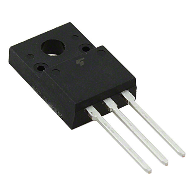
FDPF8N60ZUT N-Channel 600V 6.5A MOSFET Equivalent & Substitute Parts
Part Overview
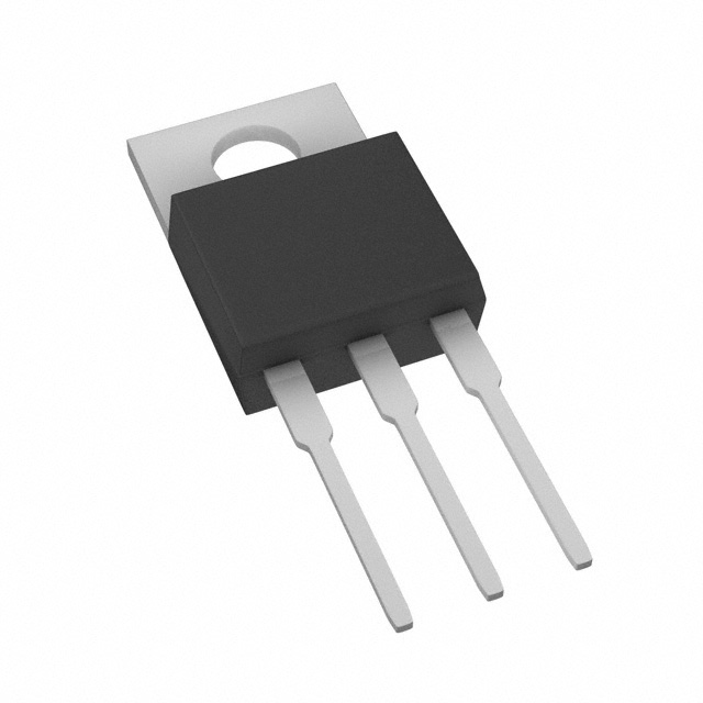
The FDPF8N60ZUT is an N-Channel 600V 6.5A MOSFET manufactured by onsemi in the UniFET™ series, housed in a Through Hole TO-220F-3 package. This device is classified as Obsolete, making identification of functionally equivalent alternatives necessary for ongoing design support and production continuity. The part delivers 34.5W maximum power dissipation and operates across a temperature range of -55°C to 150°C (TJ).
Substiute Parts
Key Parameters
| Parameter | Value | Unit |
|---|---|---|
| Drain to Source Voltage (Vdss) | 600 | V |
| Continuous Drain Current (Id) @ 25°C | 6.5 | A (Tc) |
| On-State Resistance (Rds On Max) @ Id, Vgs | 1.35 | Ohm @ 3.25A, 10V |
| Gate Threshold Voltage (Vgs(th) Max) @ Id | 5 | V @ 250µA |
| Gate Charge (Qg Max) @ Vgs | 26 | nC @ 10V |
| Maximum Gate Voltage (Vgs Max) | ±30 | V |
| Input Capacitance (Ciss Max) @ Vds | 1265 | pF @ 25V |
| Power Dissipation (Max) | 34.5 | W (Tc) |
| Operating Temperature Range | -55 to 150 | °C (TJ) |
| Mounting Type | Through Hole | — |
| Package | TO-220-3 Full Pack | — |
| RoHS Status | ROHS3 Compliant | — |
Substitute Part Grouping Explanation
Substitution of the FDPF8N60ZUT is determined by alignment across the following critical electrical and mechanical parameters:
Electrical Compatibility Criteria:
- Drain to Source Voltage (Vdss) must equal or exceed 600V
- Continuous Drain Current (Id) must equal or exceed 6.5A at 25°C
- On-State Resistance (Rds On) must not significantly degrade circuit performance
- Gate Threshold Voltage (Vgs(th)) must remain within compatible operating ranges
- Maximum Gate Voltage (Vgs Max) must support ±30V or greater
- Operating Temperature Range must span -55°C to 150°C (TJ)
Mechanical Compatibility Criteria:
- Mounting Type: Through Hole (preferred for direct replacement)
- Package: TO-220 family variants acceptable (TO-220F-3, TO-220FP, TO-220AB, TO-220SIS)
Substitute parts are grouped into two categories: Manufacturer Recommended (optimized performance characteristics) and Similar Alternatives (equivalent electrical performance with package or series variations).
Parameter Comparison
| Parameter | FDPF8N60ZUT (Main) | FCD620N60ZF | PJP7NA60_T0_00001 | STF6N62K3 | STF6N65M2 | STF9NM60N | STP5NK60ZFP | TK5A60D(STA4,Q,M) |
|---|---|---|---|---|---|---|---|---|
| Manufacturer | onsemi | onsemi | Panjit International Inc. | STMicroelectronics | STMicroelectronics | STMicroelectronics | STMicroelectronics | Toshiba Semiconductor and Storage |
| Vdss (V) | 600 | 600 | 600 | 620 | 650 | 600 | 600 | 600 |
| Id @ 25°C (A) | 6.5 (Tc) | 7.3 (Tc) | 7 (Ta) | 5.5 (Tc) | 4 (Tc) | 6.5 (Tc) | 5 (Tc) | 5 (Ta) |
| Rds On Max (Ohm) | 1.35 @ 3.25A, 10V | 0.62 @ 3.6A, 10V | 1.2 @ 3.5A, 10V | 1.28 @ 2.8A, 10V | 1.35 @ 2A, 10V | 0.745 @ 3.25A, 10V | 1.6 @ 2.5A, 10V | 1.43 @ 2.5A, 10V |
| Vgs(th) Max (V) | 5 @ 250µA | 5 @ 250µA | 4 @ 250µA | 4.5 @ 50µA | 4 @ 250µA | 4 @ 250µA | 4.5 @ 50µA | 4.4 @ 1mA |
| Qg Max (nC) | 26 @ 10V | 36 @ 10V | 15.2 @ 10V | 34 @ 10V | 9.8 @ 10V | 17.4 @ 10V | 34 @ 10V | 16 @ 10V |
| Vgs Max (V) | ±30 | ±20 | ±30 | ±30 | ±25 | ±25 | ±30 | ±30 |
| Ciss Max (pF) | 1265 @ 25V | 1135 @ 25V | 723 @ 25V | 875 @ 50V | 226 @ 100V | 452 @ 50V | 690 @ 25V | 700 @ 25V |
| Power Dissipation Max (W) | 34.5 (Tc) | 89 (Tc) | 145 (Tc) | 30 (Tc) | 20 (Tc) | 25 (Tc) | 25 (Tc) | 35 (Tc) |
| Operating Temperature (°C) | -55 to 150 | -55 to 150 | -55 to 150 | to 150 | -55 to 150 | to 150 | -55 to 150 | to 150 |
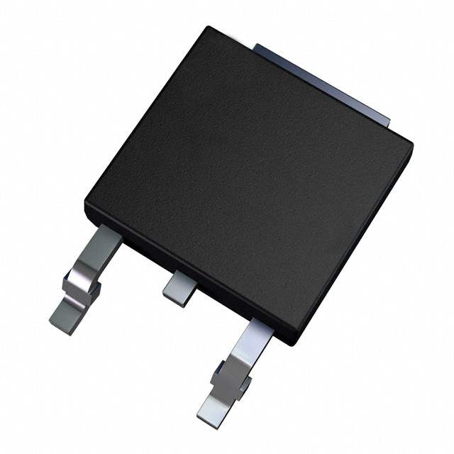
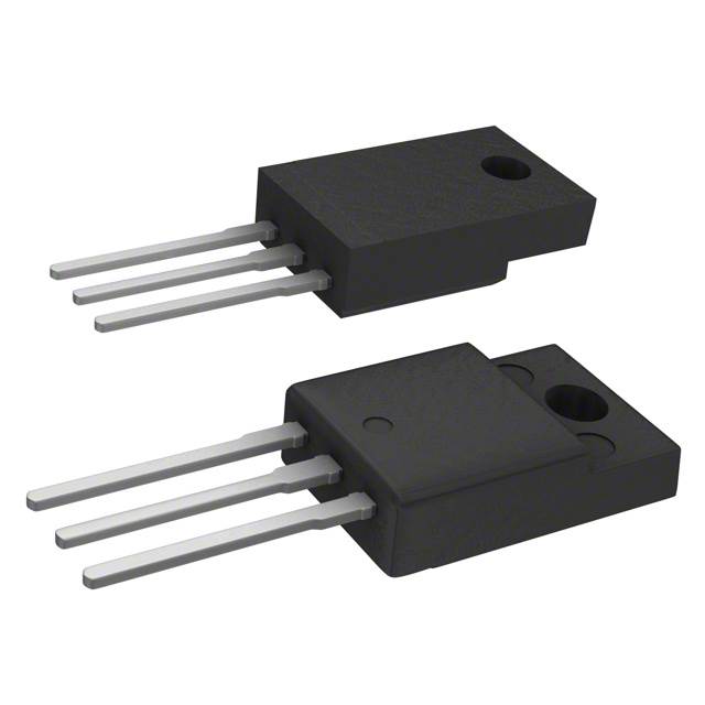
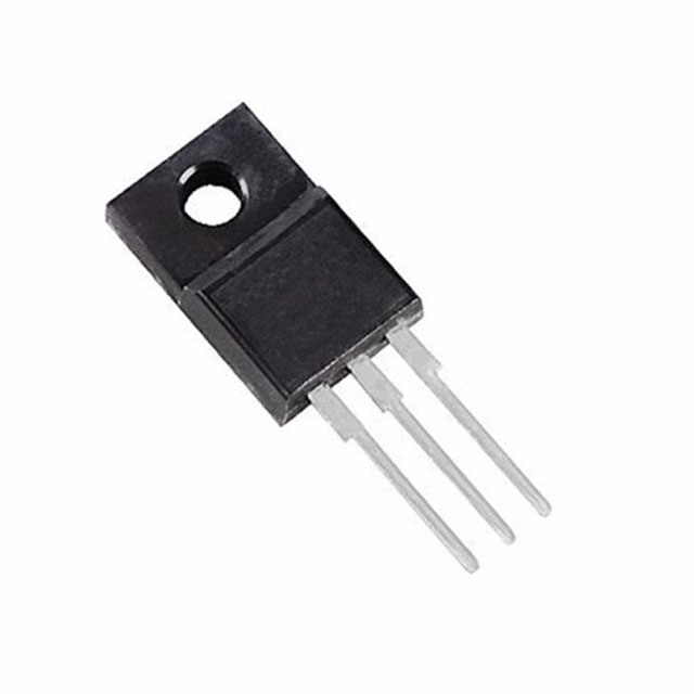
| Mounting Type | Through Hole | Surface Mount | Through Hole | Through Hole | Through Hole | Through Hole | Through Hole | Through Hole |
| Package | TO-220-3 Full Pack | TO-252-3 DPAK | TO-220-3 | TO-220-3 Full Pack | TO-220-3 Full Pack | TO-220-3 Full Pack | TO-220-3 Full Pack | TO-220-3 Full Pack |
| Product Status | Obsolete | Not For New Designs | Active | Active | Active | Active | Active | Active |
| RoHS Status | ROHS3 Compliant | ROHS3 Compliant | ROHS3 Compliant | ROHS3 Compliant | ROHS3 Compliant | ROHS3 Compliant | ROHS3 Compliant | ROHS3 Compliant |
Engineering Selection Recommendations
Manufacturer Recommended Substitute:
The FCD620N60ZF (onsemi HiPerFET™/Polar™ series) provides the closest electrical alignment with enhanced performance characteristics. This part maintains 600V Vdss rating and exceeds the 6.5A continuous drain current requirement at 7.3A. The Rds On is significantly improved at 0.62 Ohm, reducing conduction losses. However, this part is classified as "Not For New Designs" and uses Surface Mount packaging (TO-252AA DPAK), requiring PCB layout modifications from the original Through Hole design. Maximum gate voltage is limited to ±20V compared to the original ±30V specification.
Primary Through Hole Alternatives (Active Product Status):
STF9NM60N (STMicroelectronics MDmesh™ II series) is the optimal direct replacement for new designs. It matches the 600V Vdss and 6.5A Id specifications exactly, maintains Through Hole TO-220FP packaging, and is classified as Active. The Rds On of 0.745 Ohm provides superior performance compared to the original 1.35 Ohm. Gate charge is reduced to 17.4 nC, improving switching efficiency. Operating temperature range extends to 150°C (TJ). Maximum gate voltage is ±25V.
PJP7NA60_T0_00001 (Panjit International Inc.) offers Through Hole TO-220AB packaging with 7A continuous drain current, exceeding the 6.5A requirement. Rds On of 1.2 Ohm is comparable to the original specification. Gate charge is reduced to 15.2 nC. Power dissipation capability is 145W (Tc), significantly higher than the original 34.5W. This part maintains ±30V maximum gate voltage and full -55°C to 150°C operating range. Product status is Active.
STP5NK60ZFP (STMicroelectronics SuperMESH™ series) provides Through Hole TO-220FP packaging with 5A continuous drain current. While this represents a reduction from the original 6.5A specification, the Rds On of 1.6 Ohm and gate charge of 34 nC remain within acceptable operating parameters for applications not requiring full current capacity. This part is Active and maintains full -55°C to 150°C operating range with ±30V maximum gate voltage.
Secondary Alternatives (Reduced Current Capacity):
STF6N62K3 (STMicroelectronics SuperMESH3™) and STF6N65M2 (STMicroelectronics MDmesh™) are suitable only for applications where continuous drain current requirements do not exceed 5.5A and 4A respectively. Both maintain Through Hole packaging and are classified as Active. These parts are appropriate for lower-power circuit implementations.
TK5A60D(STA4,Q,M) (Toshiba π-MOSVII series) provides Through Hole TO-220SIS packaging with 5A continuous drain current. Rds On of 1.43 Ohm and gate charge of 16 nC are favorable. Power dissipation is 35W (Tc), comparable to the original specification. This part is Active and maintains ±30V maximum gate voltage.
Compliance and Certification:
All substitute parts listed are ROHS3 Compliant and REACH Unaffected, matching the original part's regulatory status. All parts carry EAR99 ECCN classification and 8541.29.0095 HTSUS code.
Frequently Asked Questions (FAQ)
Q: Can the FCD620N60ZF be used as a direct replacement for the FDPF8N60ZUT?
A: The FCD620N60ZF provides electrical equivalence in voltage and current ratings but requires design modifications. The primary limitation is packaging: FCD620N60ZF uses Surface Mount TO-252AA (DPAK) while the original uses Through Hole TO-220F-3. Additionally, maximum gate voltage is reduced from ±30V to ±20V. This part is classified as "Not For New Designs," limiting its suitability for ongoing production.
Q: Which substitute offers the best direct replacement for Through Hole applications?
A: The STF9NM60N provides the most direct replacement for Through Hole applications. It matches the 600V Vdss and 6.5A Id specifications exactly, uses Through Hole TO-220FP packaging, and is classified as Active. Performance is improved with lower Rds On (0.745 Ohm vs. 1.35 Ohm) and reduced gate charge (17.4 nC vs. 26 nC).
Q: What are the implications of using a substitute with lower continuous drain current?
A: Substitutes with lower Id ratings (such as STP5NK60ZFP at 5A or STF6N62K3 at 5.5A) are suitable only for applications where the actual circuit current demand does not exceed the substitute's rating. Using an undersized device in a circuit requiring 6.5A will result in thermal stress, reduced device lifetime, and potential failure. Circuit current requirements must be verified before selecting a lower-rated substitute.
Q: Are all substitute parts RoHS compliant?
A: Yes. All substitute parts listed are ROHS3 Compliant, matching the original FDPF8N60ZUT specification. All parts are also REACH Unaffected.
Q: What is the significance of the difference in gate charge (Qg) between the original and substitutes?
A: Gate charge affects switching speed and driver circuit requirements. Lower gate charge (such as STF6N65M2 at 9.8 nC or TK5A60D at 16 nC) reduces switching losses and allows faster switching transitions. Higher gate charge (such as STF6N62K3 at 34 nC) requires more driver current but may provide improved noise immunity. The original FDPF8N60ZUT at 26 nC represents a mid-range value. Substitutes with significantly different Qg values may require driver circuit evaluation.
Q: Can I use a substitute with higher Vdss rating?
A: Yes. Substitutes with higher Vdss ratings (such as STF6N65M2 at 650V) are fully compatible and provide additional voltage margin. Higher voltage ratings do not degrade performance in circuits operating at 600V or below. However, higher voltage devices typically exhibit increased on-state resistance and input capacitance, which may affect circuit efficiency and switching characteristics.
Q: What is the difference between Tc and Ta temperature specifications?
A: Tc (case temperature) and Ta (ambient temperature) represent different measurement points. Tc is measured at the device case and is typically lower than Ta under the same operating conditions. Specifications using Tc are generally more conservative. The original FDPF8N60ZUT uses Tc for current rating (6.5A Tc), while some substitutes use Ta (such as PJP7NA60_T0_00001 at 7A Ta). Both measurement methods are valid; circuit thermal design must account for the specified measurement point.
Q: Are there any substitutes suitable for new design implementations?
A: Yes. STF9NM60N, PJP7NA60_T0_00001, STF6N62K3, STF6N65M2, STP5NK60ZFP, and TK5A60D(STA4,Q,M) are all classified as Active and suitable for new designs. The FCD620N60ZF is classified as "Not For New Designs" and should be avoided for new implementations. The original FDPF8N60ZUT is Obsolete and should not be used in new designs.
Q: What packaging considerations apply when selecting a substitute?
A: The original FDPF8N60ZUT uses Through Hole TO-220F-3 packaging. All recommended substitutes except FCD620N60ZF also use Through Hole TO-220 family packages (TO-220FP, TO-220AB, TO-220SIS), allowing direct PCB mounting without layout modifications. The FCD620N60ZF uses Surface Mount TO-252AA (DPAK) packaging, which requires different PCB footprint and assembly process. Through Hole substitutes are preferred for direct replacement scenarios.
Q: How do I determine if a lower-current substitute is acceptable for my application?
A: Review the actual circuit current demand under all operating conditions, including transient and fault conditions. Compare this demand against the substitute's continuous drain current rating. The substitute's rating must exceed the maximum circuit current by a safety margin. Additionally, verify that the substitute's Rds On and power dissipation characteristics do not cause excessive thermal stress. Thermal analysis of the PCB layout and heat sink design is required.
Alternative Parts

SJ6012L2TP
Littelfuse Inc.
6 Alternative Parts

JMK107BBJ476MA-RE
Taiyo Yuden
10 Alternative Parts

GMK107BBJ475MA-T
Taiyo Yuden
5 Alternative Parts
SJ6020N2ARP
Littelfuse Inc.
3 Alternative Parts
SJ6025R2ATP
Littelfuse Inc.
4 Alternative Parts

2474-05L
API Delevan Inc.
1 Alternative Parts

4590R-684K
API Delevan Inc.
1 Alternative Parts

CM6560R-334
API Delevan Inc.
1 Alternative Parts

CM6460-104
API Delevan Inc.
1 Alternative Parts

5526-12
API Delevan Inc.
1 Alternative Parts