


Request Quote
(Ships tomorrow)
FDP79N15 Equivalent & Substitute Parts
Part Overview
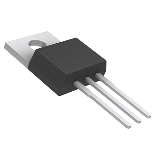
The FDP79N15 is an N-Channel MOSFET manufactured by onsemi, rated for 150V drain-to-source voltage with a continuous drain current of 79A at 25°C. This device is packaged in a Through Hole TO-220-3 configuration and is designed for high-current switching applications requiring robust thermal performance at 463W maximum power dissipation.
The FDP79N15 is classified as Obsolete. Locating equivalent substitute parts is necessary to maintain design continuity, ensure supply chain availability, and support ongoing production requirements for applications currently utilizing this component.
Substiute Parts
Key Parameters
| Parameter | Value | Unit |
|---|---|---|
| Drain to Source Voltage (Vdss) | 150 | V |
| Continuous Drain Current (Id) @ 25°C | 79 | A |
| On-State Resistance (Rds On Max) @ Id, Vgs | 30 mOhm @ 39.5A, 10V | mOhm |
| Gate Threshold Voltage (Vgs(th) Max) @ Id | 5 | V @ 250µA |
| Gate Charge (Qg Max) @ Vgs | 73 | nC @ 10V |
| Maximum Gate Voltage (Vgs Max) | ±30 | V |
| Input Capacitance (Ciss Max) @ Vds | 3410 | pF @ 25V |
| Power Dissipation (Max) | 463 | W |
| Operating Temperature Range | -55 to 150 | °C |
| Package Type | TO-220-3 | Through Hole |
| Series | UniFET™ |
Substitute Part Grouping Explanation
Substitution of the FDP79N15 is determined by strict electrical and mechanical parameter matching within the N-Channel MOSFET category. The following parameters establish substitution eligibility:
Primary Matching Criteria:
- Drain to Source Voltage (Vdss): 150V minimum
- Continuous Drain Current (Id): Rated for applications requiring 79A or greater
- On-State Resistance (Rds On): Maximum 30 mOhm at specified gate voltage
- Gate Threshold Voltage (Vgs(th)): Within acceptable switching range
- Package Type: Through Hole TO-220 configuration
- Operating Temperature Range: Minimum -55°C to 150°C
Secondary Compatibility Factors:
- Gate Charge (Qg): Affects driver circuit requirements
- Input Capacitance (Ciss): Influences switching speed and gate drive design
- Maximum Gate Voltage (Vgs Max): Must accommodate existing gate drive circuits
- Power Dissipation Rating: Thermal management capability
The PSMN030-150P,127 from Nexperia USA Inc. meets the primary electrical criteria for substitution, though with specific trade-offs in current rating and power dissipation that must be evaluated for the target application.
Parameter Comparison
| Parameter | FDP79N15 (onsemi) | PSMN030-150P,127 (Nexperia) | Match Status |
|---|---|---|---|
| Drain to Source Voltage (Vdss) | 150 V | 150 V | Matched |
| Continuous Drain Current (Id) @ 25°C | 79 A | 55.5 A | Substitute Lower |
| On-State Resistance (Rds On Max) @ Id, Vgs | 30 mOhm @ 39.5A, 10V | 30 mOhm @ 25A, 10V | Equivalent |
| Gate Threshold Voltage (Vgs(th) Max) @ Id | 5 V @ 250µA | 4 V @ 1mA | Substitute Lower |
| Gate Charge (Qg Max) @ Vgs | 73 nC @ 10V | 98 nC @ 10V | Substitute Higher |
| Maximum Gate Voltage (Vgs Max) | ±30 V | ±20 V | Substitute Lower |
| Input Capacitance (Ciss Max) @ Vds | 3410 pF @ 25V | 3680 pF @ 25V | Substitute Higher |
| Power Dissipation (Max) | 463 W | 250 W | Substitute Lower |
| Operating Temperature Range | -55 to 150 °C | -55 to 175 °C | Substitute Extended |
| Package Type | TO-220-3 | TO-220AB | Compatible |
| Product Status | Obsolete | Active | Substitute Active |
Engineering Selection Recommendations
Product Status Consideration: The FDP79N15 is classified as Obsolete, making the PSMN030-150P,127 a viable active alternative from Nexperia USA Inc. The substitute part maintains Active product status, ensuring long-term availability and continued manufacturer support.
Compliance and Certification: The PSMN030-150P,127 is RoHS3 Compliant, whereas the FDP79N15 does not specify RoHS compliance. Both parts are REACH Unaffected and classified under ECCN EAR99, maintaining equivalent regulatory standing for export and distribution.
Electrical Compatibility: The PSMN030-150P,127 maintains the 150V Vdss rating and equivalent 30 mOhm Rds On specification. However, the continuous drain current is reduced from 79A to 55.5A, and maximum power dissipation decreases from 463W to 250W. These reductions require verification that the target application does not demand the full current or thermal capacity of the original FDP79N15.
Gate Drive Compatibility: The substitute part features a lower maximum gate voltage (±20V versus ±30V) and higher gate charge (98 nC versus 73 nC). Existing gate drive circuits must be confirmed compatible with these parameters.
Thermal Management: The reduced power dissipation rating of the PSMN030-150P,127 necessitates evaluation of thermal design margins in the target application. Applications operating near the 463W dissipation limit of the FDP79N15 may require design modification.
Temperature Range: The PSMN030-150P,127 offers an extended operating temperature range (-55°C to 175°C versus -55°C to 150°C), providing additional thermal margin in high-temperature environments.
Frequently Asked Questions (FAQ)
Q: Can the PSMN030-150P,127 directly replace the FDP79N15 in all applications?
A: Direct replacement is not universal. The PSMN030-150P,127 is suitable for applications where continuous drain current does not exceed 55.5A and power dissipation remains below 250W. Applications requiring the full 79A current rating or 463W thermal capacity require design modification or alternative substitutes.
Q: What is the significance of the different gate charge specifications?
A: The PSMN030-150P,127 requires higher gate charge (98 nC versus 73 nC) to achieve full on-state conduction. Gate driver circuits must deliver sufficient charge within the switching cycle. Existing drivers designed for the FDP79N15 may require recalibration or replacement to accommodate the higher charge requirement.
Q: Are the TO-220-3 and TO-220AB packages mechanically interchangeable?
A: Both packages are Through Hole TO-220 variants with identical pin spacing and mounting footprints. Mechanical and thermal interface compatibility is maintained. Pin assignment and electrical function remain consistent between the two package designations.
Q: How does the lower maximum gate voltage of the PSMN030-150P,127 affect circuit design?
A: The PSMN030-150P,127 specifies ±20V maximum gate voltage compared to ±30V for the FDP79N15. Gate drive circuits must ensure gate voltage does not exceed ±20V to prevent device damage. Existing circuits operating at ±30V require modification or voltage limiting.
Q: What is the impact of higher input capacitance on switching performance?
A: The PSMN030-150P,127 exhibits higher input capacitance (3680 pF versus 3410 pF). This increases gate charge requirements and may extend switching transition times. High-frequency switching applications must verify that gate driver slew rate remains adequate for the target switching frequency.
Q: Is the PSMN030-150P,127 suitable for high-temperature applications?
A: The extended operating temperature range of the PSMN030-150P,127 (-55°C to 175°C versus -55°C to 150°C) provides additional margin for high-temperature environments. However, power dissipation derating at elevated temperatures must be confirmed against application thermal requirements.
Q: What inventory considerations apply to these parts?
A: The FDP79N15 has 1728 pieces in stock as new original inventory. The PSMN030-150P,127 has 836 pieces available. Both parts are available for immediate procurement, though the FDP79N15 inventory is finite due to obsolete status.
Alternative Parts

SJ6012L2TP
Littelfuse Inc.
6 Alternative Parts

JMK107BBJ476MA-RE
Taiyo Yuden
10 Alternative Parts

GMK107BBJ475MA-T
Taiyo Yuden
5 Alternative Parts
SJ6020N2ARP
Littelfuse Inc.
3 Alternative Parts
SJ6025R2ATP
Littelfuse Inc.
4 Alternative Parts

2474-05L
API Delevan Inc.
1 Alternative Parts

4590R-684K
API Delevan Inc.
1 Alternative Parts

CM6560R-334
API Delevan Inc.
1 Alternative Parts

CM6460-104
API Delevan Inc.
1 Alternative Parts

5526-12
API Delevan Inc.
1 Alternative Parts