


Request Quote
(Ships tomorrow)
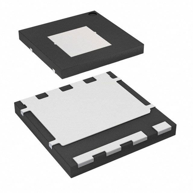
FDMT800152DC N-Channel MOSFET 150V Equivalent & Substitute Parts
Part Overview
The FDMT800152DC is an N-Channel MOSFET manufactured by onsemi, featuring 150V drain-to-source voltage rating and dual-channel configuration in a Dual Cool™88 surface mount package. This device is classified as Active product status and is designed for high-current switching applications requiring efficient thermal management. Substitute parts are identified when equivalent electrical performance parameters and mechanical compatibility are required for design flexibility, inventory management, or supply chain continuity.
Substiute Parts
Key Parameters
| Parameter | Value | Unit |
|---|---|---|
| Drain to Source Voltage (Vdss) | 150 | V |
| Continuous Drain Current @ 25°C (Ta) | 13 | A |
| Continuous Drain Current @ 25°C (Tc) | 72 | A |
| Rds On (Max) @ Id, Vgs | 9 mOhm @ 13A, 10V | mOhm |
| Gate Charge (Qg) @ Vgs | 83 | nC @ 10V |
| Vgs(th) (Max) @ Id | 4 | V @ 250µA |
| Operating Temperature Range | -55 to 150 | °C (TJ) |
| Mounting Type | Surface Mount | - |
| Package Type | 8-PowerVDFN (Dual Cool™88) | - |
| FET Type | N-Channel | - |
| Technology | MOSFET (Metal Oxide) | - |
Substitute Part Grouping Explanation
Substitute parts for the FDMT800152DC are qualified based on the following electrical and mechanical criteria:
Primary Substitution Criteria:
- Drain to Source Voltage (Vdss): 150V (exact match required)
- FET Type: N-Channel (exact match required)
- Technology: MOSFET (Metal Oxide) (exact match required)
- Operating Temperature Range: -55°C to 150°C (TJ) (exact match required)
- Mounting Type: Surface Mount (exact match required)
- RoHS3 Compliance: Required
- Moisture Sensitivity Level (MSL): 1 (Unlimited) (exact match required)
Secondary Compatibility Parameters:
- Continuous Drain Current (Id) @ 25°C: Substitute must meet or exceed 13A (Ta) and 72A (Tc)
- Rds On (Max): Substitute must not exceed 9 mOhm @ specified Id and Vgs conditions
- Gate Charge (Qg): Lower values indicate improved switching performance
- Vgs(th) (Max): Threshold voltage within ±20V gate voltage specification
- Input Capacitance (Ciss): Lower values reduce gate drive requirements
The identified substitutes (AONS66520 and AONS66521) satisfy all primary criteria and demonstrate equivalent or superior electrical performance within the secondary parameters.
Parameter Comparison
| Parameter | FDMT800152DC (onsemi) | AONS66520 (Alpha & Omega) | AONS66521 (Alpha & Omega) | Unit |
|---|---|---|---|---|
| Drain to Source Voltage (Vdss) | 150 | 150 | 150 | V |
| FET Type | N-Channel | N-Channel | N-Channel | - |
| Technology | MOSFET (Metal Oxide) | MOSFET (Metal Oxide) | MOSFET (Metal Oxide) | - |
| Continuous Drain Current @ 25°C (Ta) | 13 | 17 | 16 | A |
| Continuous Drain Current @ 25°C (Tc) | 72 | 100 | 100 | A |
| Rds On (Max) @ Id, Vgs | 9 @ 13A, 10V | 9.5 @ 20A, 10V | 9.8 @ 20A, 10V | mOhm |
| Gate Charge (Qg) @ Vgs | 83 @ 10V | 65 @ 10V | 45 @ 10V | nC |
| Vgs(th) (Max) @ Id | 4 @ 250µA | 2.6 @ 250µA | 4.5 @ 250µA | V |
| Vgs (Max) | ±20 | ±20 | ±20 | V |
| Input Capacitance (Ciss) @ Vds | 5875 @ 75V | 3200 @ 75V | 2600 @ 75V | pF |
| Operating Temperature Range | -55 to 150 | -55 to 150 | -55 to 150 | °C (TJ) |
| Mounting Type | Surface Mount | Surface Mount | Surface Mount | - |
| Package Type | 8-PowerVDFN | 8-DFN (5x6) | 8-DFN (5x6) | - |
| RoHS3 Compliance | Yes | Yes | Yes | - |
| MSL Rating | 1 (Unlimited) | 1 (Unlimited) | 1 (Unlimited) | - |
Engineering Selection Recommendations
FDMT800152DC (onsemi) - Primary Part
The FDMT800152DC remains the primary selection when onsemi component qualification is required or when the Dual Cool™88 package geometry is specified in the design. This device is Active product status with full RoHS3 compliance and MSL 1 rating, supporting unlimited moisture exposure without baking requirements.
AONS66520 (Alpha & Omega Semiconductor Inc.) - Substitute Option
The AONS66520 qualifies as a direct substitute with superior electrical performance characteristics. This device provides 17A continuous drain current (Ta) and 100A (Tc), exceeding the FDMT800152DC ratings. Gate charge is reduced to 65 nC, and input capacitance is 3200 pF, both lower than the primary part. The 8-DFN (5x6) package is mechanically compatible with surface mount assembly processes. Active product status and RoHS3 compliance are confirmed. Inventory availability is 5410 units.
AONS66521 (Alpha & Omega Semiconductor Inc.) - Substitute Option
The AONS66521 qualifies as a direct substitute with the highest performance efficiency among the three options. This device provides 16A continuous drain current (Ta) and 100A (Tc). Gate charge is minimized at 45 nC, and input capacitance is 2600 pF, the lowest of all three parts. The 8-DFN (5x6) package is mechanically compatible with surface mount assembly processes. Active product status and RoHS3 compliance are confirmed. Inventory availability is 22988 units, the highest among all options.
Selection Basis:
All three parts satisfy mandatory electrical and mechanical substitution criteria. Selection between AONS66520 and AONS66521 depends on gate drive circuit capability and switching frequency requirements. The AONS66521 exhibits the lowest gate charge and input capacitance, reducing gate driver power dissipation and enabling higher switching frequencies. Both Alpha & Omega parts demonstrate superior thermal performance (215W Tc vs. 113W Tc) compared to the primary part.
Frequently Asked Questions (FAQ)
Q: Can AONS66520 or AONS66521 be used as direct replacements for FDMT800152DC in existing designs?
A: Yes, both Alpha & Omega parts satisfy all primary substitution criteria: 150V Vdss, N-Channel MOSFET technology, -55°C to 150°C operating range, surface mount configuration, RoHS3 compliance, and MSL 1 rating. Electrical performance parameters meet or exceed FDMT800152DC specifications. PCB layout modifications may be required due to package geometry differences (8-PowerVDFN vs. 8-DFN 5x6).
Q: What are the package geometry differences between FDMT800152DC and the substitute parts?
A: The FDMT800152DC uses an 8-PowerVDFN (Dual Cool™88) package, while AONS66520 and AONS66521 use 8-DFN (5x6) packages. Both are surface mount configurations with flat leads. Physical footprint and thermal pad dimensions differ. PCB artwork and assembly process parameters require verification before implementation.
Q: Are there thermal performance differences between these parts?
A: Yes. The FDMT800152DC is rated for 3.2W (Ta) and 113W (Tc) power dissipation. Both AONS66520 and AONS66521 are rated for 6.2W (Ta) and 215W (Tc), indicating superior thermal performance. Lower junction temperatures are achievable with substitute parts under equivalent power dissipation conditions.
Q: Which substitute part has the lowest gate charge?
A: AONS66521 has the lowest gate charge at 45 nC @ 10V, compared to 65 nC for AONS66520 and 83 nC for FDMT800152DC. Lower gate charge reduces gate driver power dissipation and enables higher switching frequencies in applications with limited gate drive capability.
Q: Do all three parts have identical moisture sensitivity requirements?
A: Yes. All three parts are rated MSL 1 (Unlimited), indicating no moisture sensitivity. Components can be stored and handled without baking requirements, simplifying inventory management and assembly logistics.
Q: What is the significance of lower input capacitance in AONS66521?
A: Input capacitance (Ciss) of 2600 pF in AONS66521 versus 5875 pF in FDMT800152DC reduces gate drive circuit loading. Lower Ciss decreases gate driver current requirements and enables faster switching transitions, improving overall circuit efficiency in high-frequency applications.
Q: Are all parts RoHS3 compliant?
A: Yes. FDMT800152DC, AONS66520, and AONS66521 are all RoHS3 compliant. REACH status is unaffected for all three parts, and ECCN classification is EAR99 for all devices.
Q: Can gate threshold voltage differences affect circuit operation?
A: Gate threshold voltage (Vgs(th)) differs among the three parts: FDMT800152DC at 4V, AONS66520 at 2.6V, and AONS66521 at 4.5V. These variations are within the ±20V gate voltage specification and do not prevent substitution. Gate drive circuit design should accommodate the specified Vgs(th) range for reliable switching operation.
Alternative Parts

SJ6012L2TP
Littelfuse Inc.
6 Alternative Parts

JMK107BBJ476MA-RE
Taiyo Yuden
10 Alternative Parts

GMK107BBJ475MA-T
Taiyo Yuden
5 Alternative Parts
SJ6020N2ARP
Littelfuse Inc.
3 Alternative Parts
SJ6025R2ATP
Littelfuse Inc.
4 Alternative Parts

2474-05L
API Delevan Inc.
1 Alternative Parts

4590R-684K
API Delevan Inc.
1 Alternative Parts

CM6560R-334
API Delevan Inc.
1 Alternative Parts

CM6460-104
API Delevan Inc.
1 Alternative Parts

5526-12
API Delevan Inc.
1 Alternative Parts