


Request Quote
(Ships tomorrow)
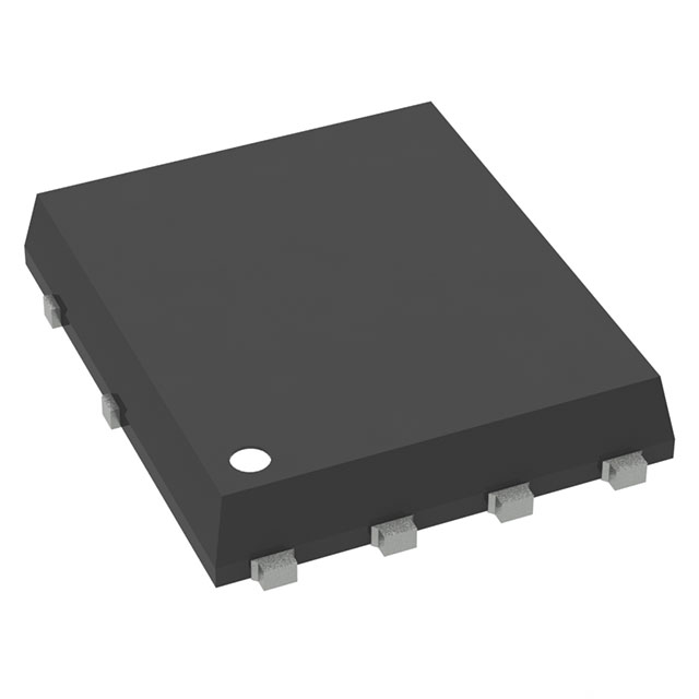
FDMS9409L-F085 Equivalent & Substitute Parts
Part Overview
The FDMS9409L-F085 is an N-Channel MOSFET manufactured by onsemi, rated for 40V drain-to-source voltage with 65A continuous drain current at 25°C. This device is housed in an 8-PQFN (5x6) surface mount package and is qualified to AEC-Q101 automotive standards. The part is currently classified as obsolete, necessitating identification of functionally equivalent alternatives for ongoing design support and procurement continuity.
Substiute Parts
Key Parameters
| Parameter | Value | Unit |
|---|---|---|
| Drain-to-Source Voltage (Vdss) | 40 | V |
| Continuous Drain Current (Id) @ 25°C | 65 | A (Tc) |
| On-Resistance (Rds On Max) @ 65A, 10V | 2.8 | mOhm |
| Gate Threshold Voltage (Vgs(th) Max) @ 250µA | 3 | V |
| Gate Charge (Qg Max) @ 10V | 70 | nC |
| Power Dissipation (Max) | 100 | W (Tj) |
| Operating Temperature Range | -55 to 175 | °C (TJ) |
| Package Type | 8-PQFN (5x6) | Surface Mount |
| Automotive Grade | AEC-Q101 | Qualified |
Substitute Part Grouping Explanation
Substitution of the FDMS9409L-F085 is determined by electrical and mechanical compatibility across the following critical parameters:
Electrical Compatibility Criteria:
- Drain-to-Source Voltage (Vdss): Must equal or exceed 40V
- On-Resistance (Rds On): Must not exceed 2.8mOhm at rated conditions to maintain thermal and efficiency performance
- Gate Threshold Voltage (Vgs(th)): Must be compatible with existing gate drive circuitry
- Operating Temperature Range: Must support -55°C to 175°C (TJ)
Mechanical Compatibility Criteria:
- Surface mount technology required
- Package footprint compatibility with 5x6mm form factor
- Lead count and pinout configuration
Compliance Criteria:
- AEC-Q101 automotive qualification required
- REACH compliance status
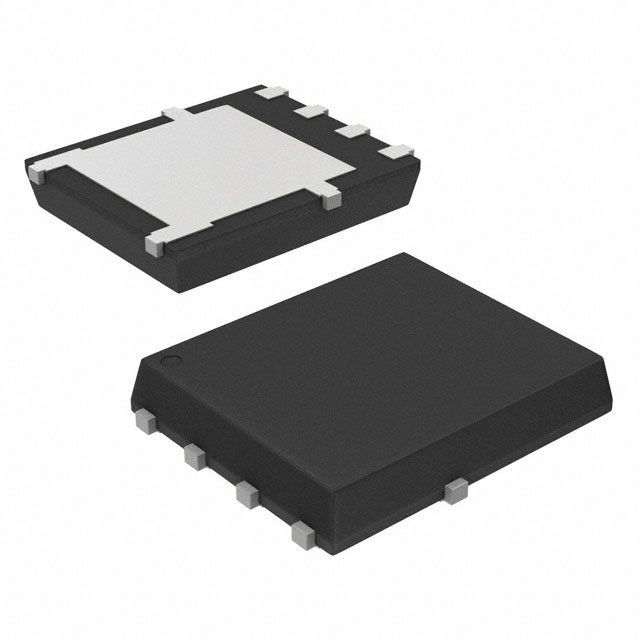
The NVMFS5C450NLAFT1G meets these substitution criteria through equivalent voltage rating, compatible on-resistance specification, matching temperature range, automotive qualification, and compatible surface mount packaging.
Parameter Comparison
| Parameter | FDMS9409L-F085 | NVMFS5C450NLAFT1G | Unit |
|---|---|---|---|
| Manufacturer | onsemi | onsemi | — |
| FET Type | N-Channel | N-Channel | — |
| Technology | MOSFET (Metal Oxide) | MOSFET (Metal Oxide) | — |
| Drain-to-Source Voltage (Vdss) | 40 | 40 | V |
| Continuous Drain Current (Id) @ 25°C | 65 | 110 | A (Tc) |
| On-Resistance (Rds On Max) @ 10V | 2.8 @ 65A | 2.8 @ 40A | mOhm |
| Gate Threshold Voltage (Vgs(th) Max) @ 250µA | 3 | 2 | V |
| Gate Charge (Qg Max) @ 10V | 70 | 35 | nC |
| Input Capacitance (Ciss Max) @ 20V | 3360 | 2100 | pF |
| Power Dissipation (Max) | 100 | 68 | W (Tj) |
| Operating Temperature Range | -55 to 175 | -55 to 175 | °C (TJ) |
| Mounting Type | Surface Mount | Surface Mount | — |
| Package Type | 8-PQFN (5x6) | 5-DFN (5x6) (8-SOFL) | — |
| Automotive Grade | AEC-Q101 | AEC-Q101 | — |
| Product Status | Obsolete | Active | — |
Engineering Selection Recommendations
The NVMFS5C450NLAFT1G is a qualified substitute for the obsolete FDMS9409L-F085 based on the following engineering factors:
Voltage and Current Ratings: Both devices are rated for 40V Vdss. The NVMFS5C450NLAFT1G provides higher continuous drain current (110A versus 65A), which offers design margin and does not create incompatibility in applications designed for the original part.
On-Resistance Performance: Both devices specify 2.8mOhm maximum on-resistance at 10V gate drive, ensuring equivalent switching losses and thermal performance in the application circuit.
Gate Drive Compatibility: The NVMFS5C450NLAFT1G features a lower gate threshold voltage (2V versus 3V) and reduced gate charge (35nC versus 70nC), resulting in faster switching response and reduced gate drive power requirements. These characteristics are compatible with existing gate drive circuits designed for the FDMS9409L-F085.
Thermal and Reliability: Both devices operate across the identical temperature range (-55°C to 175°C TJ) and hold AEC-Q101 automotive qualification, ensuring equivalent reliability and compliance in automotive applications.
Product Status: The NVMFS5C450NLAFT1G is active in production, providing long-term availability and supply chain stability compared to the obsolete FDMS9409L-F085.
Package Consideration: The NVMFS5C450NLAFT1G uses a 5-DFN (5x6) package versus the 8-PQFN (5x6) of the original part. Both packages maintain the 5x6mm footprint; however, the lead count and pinout differ. PCB layout and schematic verification is required to confirm compatibility with existing designs.
Frequently Asked Questions (FAQ)
Q: Can the NVMFS5C450NLAFT1G be used as a direct replacement for the FDMS9409L-F085?
A: Electrical substitution is valid based on voltage rating, on-resistance, and thermal specifications. However, mechanical substitution requires verification of package pinout and PCB footprint compatibility, as the NVMFS5C450NLAFT1G uses a 5-DFN package (5 leads) while the FDMS9409L-F085 uses an 8-PQFN package (8 leads).
Q: What are the key electrical advantages of the NVMFS5C450NLAFT1G?
A: The substitute part provides higher continuous drain current (110A versus 65A), lower gate threshold voltage (2V versus 3V), and reduced gate charge (35nC versus 70nC). These characteristics enable faster switching and reduced gate drive power consumption while maintaining equivalent on-resistance performance.
Q: Are both parts qualified for automotive applications?
A: Yes. Both the FDMS9409L-F085 and NVMFS5C450NLAFT1G hold AEC-Q101 automotive qualification and operate across the identical temperature range (-55°C to 175°C TJ), ensuring equivalent reliability for automotive-grade designs.
Q: Why is the FDMS9409L-F085 classified as obsolete?
A: The FDMS9409L-F085 is no longer in active production. The NVMFS5C450NLAFT1G represents onsemi's current-generation equivalent with improved electrical performance and active manufacturing status.
Q: What is the impact of the lower gate charge on circuit design?
A: The reduced gate charge (35nC versus 70nC) in the NVMFS5C450NLAFT1G decreases the energy required to switch the device and reduces switching time. Existing gate drive circuits designed for the FDMS9409L-F085 will operate with improved efficiency and faster response when driving the substitute part.
Q: Must the PCB layout be modified to use the NVMFS5C450NLAFT1G?
A: Yes. The package change from 8-PQFN to 5-DFN requires PCB footprint modification and schematic verification to confirm pinout compatibility. Direct PCB substitution without layout changes is not possible.
Alternative Parts

SJ6012L2TP
Littelfuse Inc.
6 Alternative Parts

JMK107BBJ476MA-RE
Taiyo Yuden
10 Alternative Parts

GMK107BBJ475MA-T
Taiyo Yuden
5 Alternative Parts
SJ6020N2ARP
Littelfuse Inc.
3 Alternative Parts
SJ6025R2ATP
Littelfuse Inc.
4 Alternative Parts

2474-05L
API Delevan Inc.
1 Alternative Parts

4590R-684K
API Delevan Inc.
1 Alternative Parts

CM6560R-334
API Delevan Inc.
1 Alternative Parts

CM6460-104
API Delevan Inc.
1 Alternative Parts

5526-12
API Delevan Inc.
1 Alternative Parts