


Request Quote
(Ships tomorrow)
FDMS5362L-F085 Equivalent & Substitute Parts
Part Overview
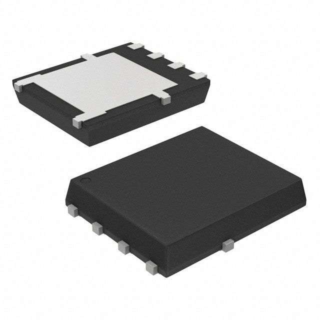
The FDMS5362L-F085 is an N-Channel 60V MOSFET manufactured by onsemi, rated for 17.6A continuous drain current at 25°C with a maximum power dissipation of 41.7W. This device is housed in a Power56 package (8-PowerVDFN) and is qualified to AEC-Q101 automotive standards. The part is currently classified as obsolete, necessitating identification of functionally equivalent alternatives for ongoing design support and procurement continuity.
Substiute Parts
Key Parameters
| Parameter | Value | Unit |
|---|---|---|
| Drain to Source Voltage (Vdss) | 60 | V |
| Continuous Drain Current (Id) @ 25°C | 17.6 | A (Tc) |
| Rds On (Max) @ Id, Vgs | 33 | mOhm @ 17.6A, 10V |
| Gate Charge (Qg) @ Vgs | 21 | nC @ 10V |
| Input Capacitance (Ciss) @ Vds | 878 | pF @ 25V |
| Power Dissipation (Max) | 41.7 | W (Tc) |
| Operating Temperature Range | -55 to 175 | °C (TJ) |
| Package Type | 8-PowerVDFN | Power56 |
| Qualification | AEC-Q101 | Automotive |
Substitute Part Grouping Explanation
Substitution of the FDMS5362L-F085 is determined by the following critical electrical and mechanical parameters:
Voltage Rating Compatibility: The substitute part must maintain the 60V Vdss rating to ensure safe operation within the same voltage domain.
Current Handling Capability: The substitute must support the required continuous drain current specification. The FDMS5362L-F085 is rated for 17.6A (Tc). Substitute parts with equal or higher current ratings at the same temperature condition are acceptable.
On-Resistance (Rds On): The substitute must not exceed the maximum on-resistance of 33mOhm at the specified gate voltage and current conditions to maintain thermal performance and power efficiency.
Gate Charge and Input Capacitance: These parameters affect switching speed and gate drive requirements. Substitutes with lower or equal values ensure compatibility with existing gate drive circuits.
Temperature Range and Thermal Rating: The substitute must support the full operating temperature range (-55°C to 175°C) and maintain adequate power dissipation capability.
Package and Mounting: Physical compatibility with the PCB layout and assembly process is required. Package type changes may necessitate board redesign.
Automotive Qualification: AEC-Q101 certification is mandatory for automotive applications.
Parameter Comparison
| Parameter | FDMS5362L-F085 | NVMFS5C680NLWFT1G | Unit |
|---|---|---|---|
| Manufacturer | onsemi | onsemi | — |
| FET Type | N-Channel | N-Channel | — |
| Drain to Source Voltage (Vdss) | 60 | 60 | V |
| Continuous Drain Current (Id) @ 25°C | 17.6 (Tc) | 21 (Tc) | A |
| Rds On (Max) @ Vgs 10V | 33 @ 17.6A | 27.5 @ 7.5A | mOhm |
| Gate Charge (Qg) @ 10V | 21 | 5.8 | nC |
| Input Capacitance (Ciss) @ 25V | 878 | 330 | pF |
| Power Dissipation (Max) @ Tc | 41.7 | 24 | W |
| Operating Temperature Range | -55 to 175 | -55 to 175 | °C (TJ) |
| Grade | Automotive | Automotive | — |
| Qualification | AEC-Q101 | AEC-Q101 | — |
| Package Type | 8-PowerVDFN (Power56) | 5-DFNW (4.9x5.9) (8-SOFL-WF) | — |
| RoHS Status | ROHS3 Compliant | ROHS3 Compliant | — |
| Moisture Sensitivity Level | 1 (Unlimited) | 1 (Unlimited) | — |
| Product Status | Obsolete | Active | — |
Engineering Selection Recommendations
NVMFS5C680NLWFT1G as Primary Substitute:
The NVMFS5C680NLWFT1G is an active production part from onsemi that meets the core electrical requirements for substitution. Both devices share identical 60V Vdss ratings and operate across the same temperature range (-55°C to 175°C). Both are AEC-Q101 qualified automotive-grade components with ROHS3 compliance and MSL 1 moisture sensitivity ratings.
The NVMFS5C680NLWFT1G provides 21A continuous drain current at Tc, exceeding the FDMS5362L-F085 specification of 17.6A. This higher current rating provides design margin for the same voltage domain. The on-resistance of 27.5mOhm at 7.5A and 10V gate voltage is lower than the FDMS5362L-F085 specification of 33mOhm at 17.6A and 10V, indicating improved efficiency characteristics.
Gate charge is significantly reduced in the substitute part (5.8nC versus 21nC), and input capacitance is substantially lower (330pF versus 878pF). These reductions improve switching performance and reduce gate drive power requirements.
Package Consideration:
The primary limitation is package incompatibility. The FDMS5362L-F085 uses an 8-PowerVDFN (Power56) package, while the NVMFS5C680NLWFT1G uses a 5-DFNW (4.9x5.9) package with wettable flank construction. This difference requires PCB layout modification and potential assembly process adjustment. The substitute part is physically smaller, which may simplify thermal management in some applications but necessitates board redesign.
Compliance and Availability:
The NVMFS5C680NLWFT1G is in active production with 1393 units in stock, ensuring long-term availability and supply chain stability. The FDMS5362L-F085 is obsolete, making the substitute the only viable path for new designs and ongoing production support.
Frequently Asked Questions (FAQ)
Q: Can the NVMFS5C680NLWFT1G directly replace the FDMS5362L-F085 without circuit modification?
A: Electrical substitution is valid. Both devices operate at 60V with compatible temperature ranges and automotive qualifications. However, package differences require PCB layout changes. The substitute's lower gate charge and input capacitance may improve circuit performance but do not require gate drive circuit redesign if the original design accommodates these parameters.
Q: What is the impact of the lower power dissipation rating in the substitute part?
A: The NVMFS5C680NLWFT1G is rated for 24W (Tc) compared to 41.7W (Tc) for the FDMS5362L-F085. This reflects the smaller package size. For applications operating within the substitute's thermal limits, this is not a limitation. Thermal analysis of the specific application is required to confirm adequate heat dissipation with the new package.
Q: Are there any gate drive compatibility concerns?
A: The substitute part has significantly lower gate charge (5.8nC versus 21nC) and input capacitance (330pF versus 878pF). Existing gate drive circuits designed for the FDMS5362L-F085 will operate with improved performance margins. No gate drive circuit modifications are necessary.
Q: What is the significance of the wettable flank feature on the substitute part?
A: The wettable flank construction on the NVMFS5C680NLWFT1G improves solder joint inspection and reliability during manufacturing. This is a manufacturing advantage with no impact on electrical performance or end-use reliability.
Q: Is the higher continuous drain current rating of the substitute part a concern?
A: No. The 21A rating of the NVMFS5C680NLWFT1G exceeds the 17.6A requirement of the original design, providing additional design margin. The application will operate within the substitute's rated specifications.
Q: What are the key differences in on-resistance specifications?
A: The FDMS5362L-F085 specifies 33mOhm at 17.6A and 10V gate voltage. The NVMFS5C680NLWFT1G specifies 27.5mOhm at 7.5A and 10V gate voltage. Direct comparison at identical current levels is not possible from the provided specifications. However, the lower on-resistance at the specified test point indicates superior conduction characteristics in the substitute part.
Q: Are both parts suitable for automotive applications?
A: Yes. Both the FDMS5362L-F085 and NVMFS5C680NLWFT1G are AEC-Q101 qualified automotive-grade components. The substitute maintains full automotive compliance and qualification status.
Alternative Parts

SJ6012L2TP
Littelfuse Inc.
6 Alternative Parts

JMK107BBJ476MA-RE
Taiyo Yuden
10 Alternative Parts

GMK107BBJ475MA-T
Taiyo Yuden
5 Alternative Parts
SJ6020N2ARP
Littelfuse Inc.
3 Alternative Parts
SJ6025R2ATP
Littelfuse Inc.
4 Alternative Parts

2474-05L
API Delevan Inc.
1 Alternative Parts

4590R-684K
API Delevan Inc.
1 Alternative Parts

CM6560R-334
API Delevan Inc.
1 Alternative Parts

CM6460-104
API Delevan Inc.
1 Alternative Parts

5526-12
API Delevan Inc.
1 Alternative Parts