


Request Quote
(Ships tomorrow)
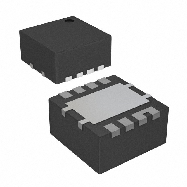
FDMS3602S Equivalent & Substitute Parts
Part Overview
The FDMS3602S is a dual N-channel MOSFET array manufactured by onsemi, designed for surface mount applications in the PowerTrench® series. This device features a 25V drain-to-source voltage rating with continuous drain current capabilities of 15A and 26A per channel, housed in an 8-PowerTDFN package. The FDMS3602S is classified as obsolete, necessitating identification of equivalent substitute components for new designs and ongoing production requirements. Substitute parts must maintain functional compatibility across voltage ratings, current handling, thermal characteristics, and mounting specifications.
Substiute Parts
Key Parameters
| Parameter | FDMS3602S |
|---|---|
| Manufacturer | onsemi |
| Configuration | 2 N-Channel (Dual) |
| Drain-to-Source Voltage (Vdss) | 25V |
| Continuous Drain Current (Id) @ 25°C | 15A, 26A |
| RDS(on) Max @ Id, Vgs | 5.6mOhm @ 15A, 10V |
| Gate Threshold Voltage (Vgs(th)) Max @ Id | 3V @ 250µA |
| Gate Charge (Qg) Max @ Vgs | 27nC @ 10V |
| Input Capacitance (Ciss) Max @ Vds | 1680pF @ 13V |
| Power Dissipation Max | 1W |
| Operating Temperature Range | -55°C to 150°C (TJ) |
| Mounting Type | Surface Mount |
| Package / Case | 8-PowerTDFN |
| FET Feature | Logic Level Gate |
| Product Status | Obsolete |
| RoHS Status | ROHS3 Compliant |
| Moisture Sensitivity Level (MSL) | 1 (Unlimited) |
Substitute Part Grouping Explanation
Substitute parts for the FDMS3602S are selected based on the following critical parameters that determine functional compatibility:
Voltage Rating Compatibility: Substitute devices must equal or exceed the 25V Vdss specification. Parts rated at higher voltages (30V) remain compatible for 25V applications.
Current Handling Capability: Substitute parts must support continuous drain current at or above the FDMS3602S specification of 15A minimum per channel. Higher current ratings provide design margin and thermal performance improvements.
Configuration: Dual N-channel (2 N-Channel) configuration is required to maintain circuit topology compatibility.
Logic Level Gate Operation: All substitutes must feature logic level gate drive capability to ensure compatibility with standard digital control signals.
Operating Temperature Range: Substitute parts must maintain the -55°C to 150°C junction temperature operating range.
Surface Mount Technology: All substitutes utilize surface mount packaging suitable for automated assembly processes.
Compliance Standards: RoHS3 compliance and MSL 1 rating are maintained across all substitute options.
Parameter Comparison
| Parameter | FDMS3602S | FDPC8016S | CSD87350Q5D |
|---|---|---|---|
| Manufacturer | onsemi | onsemi | Texas Instruments |
| Configuration | 2 N-Channel (Dual) | 2 N-Channel (Dual) Asymmetrical | 2 N-Channel (Dual) |
| Drain-to-Source Voltage (Vdss) | 25V | 25V | 30V |
| Continuous Drain Current (Id) @ 25°C | 15A, 26A | 20A, 35A | 40A |
| RDS(on) Max @ Id, Vgs | 5.6mOhm @ 15A, 10V | 3.8mOhm @ 20A, 10V | 5.9mOhm @ 20A, 8V |
| Gate Threshold Voltage (Vgs(th)) Max @ Id | 3V @ 250µA | 2.5V @ 250µA | 2.1V @ 250µA |
| Gate Charge (Qg) Max @ Vgs | 27nC @ 10V | 35nC @ 10V | 10.9nC @ 4.5V |
| Input Capacitance (Ciss) Max @ Vds | 1680pF @ 13V | 2375pF @ 13V | 1770pF @ 15V |
| Power Dissipation Max | 1W | 2.1W, 2.3W | 12W |
| Operating Temperature Range | -55°C to 150°C (TJ) | -55°C to 150°C (TJ) | -55°C to 150°C (TJ) |
| Mounting Type | Surface Mount | Surface Mount | Surface Mount |
| Package / Case | 8-PowerTDFN | 8-PowerWDFN | 8-PowerLDFN |
| FET Feature | Logic Level Gate | Logic Level Gate | Logic Level Gate |
| Product Status | Obsolete | Active | Active |
| RoHS Status | ROHS3 Compliant | ROHS3 Compliant | ROHS3 Compliant |
| Moisture Sensitivity Level (MSL) | 1 (Unlimited) | 1 (Unlimited) | 1 (Unlimited) |
Engineering Selection Recommendations
FDPC8016S (onsemi): This substitute maintains onsemi PowerTrench® series continuity with active product status. The FDPC8016S provides enhanced current handling (20A, 35A) and improved thermal performance (2.1W, 2.3W) compared to the obsolete FDMS3602S. The 25V Vdss rating matches the original specification exactly. The asymmetrical dual configuration and lower RDS(on) value (3.8mOhm @ 20A, 10V) deliver superior efficiency. Package transition from 8-PowerTDFN to 8-PowerWDFN requires PCB layout modification. This option is suitable for designs prioritizing thermal performance and supply chain continuity within the onsemi product ecosystem.
CSD87350Q5D (Texas Instruments): This substitute represents a cross-manufacturer alternative utilizing Texas Instruments NexFET™ technology. The CSD87350Q5D exceeds FDMS3602S specifications across multiple parameters: 30V Vdss rating provides 5V design margin, 40A continuous drain current offers substantial current headroom, and 12W power dissipation enables high-power applications. The lower gate threshold voltage (2.1V @ 250µA) and reduced gate charge (10.9nC @ 4.5V) improve switching performance. Package transition from 8-PowerTDFN to 8-PowerLDFN (5x6) requires PCB redesign. This option is appropriate for applications requiring enhanced thermal capability and cross-manufacturer supply diversification.
Both substitute parts maintain compliance with RoHS3 standards, MSL 1 moisture sensitivity rating, and the -55°C to 150°C operating temperature range. Product status transition from obsolete to active ensures long-term availability and supply chain stability.
Frequently Asked Questions (FAQ)
Q: Can the FDPC8016S directly replace the FDMS3602S without PCB modifications?
A: No. While both devices are onsemi PowerTrench® dual N-channel MOSFETs with 25V Vdss ratings, the package transition from 8-PowerTDFN to 8-PowerWDFN requires PCB layout modification. Pin assignments and thermal pad dimensions differ between packages.
Q: What are the key differences between the FDPC8016S and CSD87350Q5D substitutes?
A: The FDPC8016S maintains 25V Vdss matching the original FDMS3602S, while the CSD87350Q5D provides 30V Vdss. Current ratings differ: FDPC8016S delivers 20A/35A versus CSD87350Q5D at 40A. Power dissipation capabilities are 2.1W/2.3W (FDPC8016S) versus 12W (CSD87350Q5D). Package footprints differ: 8-PowerWDFN versus 8-PowerLDFN (5x6). Manufacturer differs: onsemi versus Texas Instruments.
Q: Is the CSD87350Q5D suitable for applications designed for 25V operation?
A: Yes. The CSD87350Q5D 30V Vdss rating is compatible with 25V applications. The higher voltage rating provides design margin and does not compromise functionality in 25V circuits.
Q: Do all substitute parts maintain the same operating temperature range?
A: Yes. Both FDPC8016S and CSD87350Q5D maintain the -55°C to 150°C junction temperature operating range specified for the FDMS3602S.
Q: Are there differences in gate drive requirements between the FDMS3602S and its substitutes?
A: All three devices feature logic level gate operation. Gate threshold voltages differ slightly: FDMS3602S at 3V, FDPC8016S at 2.5V, and CSD87350Q5D at 2.1V. These variations remain within standard logic level gate specifications and do not require gate drive circuit modifications.
Q: What compliance certifications apply to the substitute parts?
A: Both FDPC8016S and CSD87350Q5D are ROHS3 compliant with MSL 1 (Unlimited) moisture sensitivity rating, matching the original FDMS3602S compliance profile.
Q: How do RDS(on) values compare across the three devices?
A: FDMS3602S specifies 5.6mOhm @ 15A, 10V. FDPC8016S provides 3.8mOhm @ 20A, 10V, representing improved on-resistance. CSD87350Q5D specifies 5.9mOhm @ 20A, 8V. Lower RDS(on) values reduce conduction losses and heat generation.
Q: Are package footprint changes significant for PCB redesign?
A: Yes. The transition from 8-PowerTDFN (original) to either 8-PowerWDFN (FDPC8016S) or 8-PowerLDFN (CSD87350Q5D) requires PCB layout modification. Thermal pad dimensions and pin spacing differ between packages, necessitating updated artwork and assembly procedures.
Alternative Parts

SJ6012L2TP
Littelfuse Inc.
6 Alternative Parts

JMK107BBJ476MA-RE
Taiyo Yuden
10 Alternative Parts

GMK107BBJ475MA-T
Taiyo Yuden
5 Alternative Parts
SJ6020N2ARP
Littelfuse Inc.
3 Alternative Parts
SJ6025R2ATP
Littelfuse Inc.
4 Alternative Parts

2474-05L
API Delevan Inc.
1 Alternative Parts

4590R-684K
API Delevan Inc.
1 Alternative Parts

CM6560R-334
API Delevan Inc.
1 Alternative Parts

CM6460-104
API Delevan Inc.
1 Alternative Parts

5526-12
API Delevan Inc.
1 Alternative Parts