


Request Quote
(Ships tomorrow)
FDMD84100 Equivalent & Substitute Parts
Part Overview
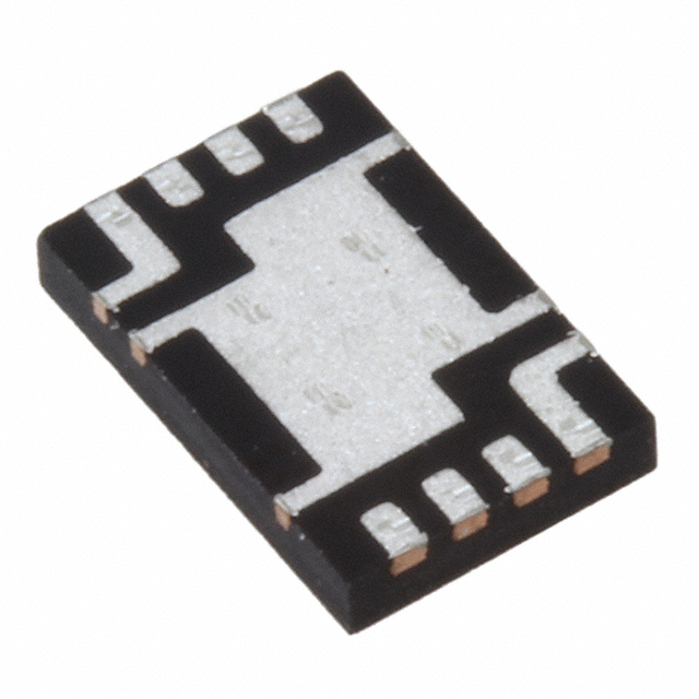
The FDMD84100 is a dual N-channel MOSFET array manufactured by onsemi, designed for power switching applications with a maximum drain-source voltage rating of 100V and continuous drain current of 7A. The device is housed in a Power 3.3x5 surface mount package and features the PowerTrench® technology platform. This part is classified as obsolete, necessitating identification of functionally equivalent alternatives for new designs and ongoing production requirements.
Substiute Parts
Key Parameters
| Parameter | Value | Unit |
|---|---|---|
| Drain to Source Voltage (Vdss) | 100 | V |
| Continuous Drain Current (Id) @ 25°C | 7 | A |
| On-Resistance (Rds On) @ Id, Vgs | 20 mOhm @ 7A, 10V | mOhm |
| Gate Threshold Voltage (Vgs(th)) @ Id | 4 | V @ 250µA |
| Gate Charge (Qg) @ Vgs | 16 | nC @ 10V |
| Input Capacitance (Ciss) @ Vds | 980 | pF @ 50V |
| Maximum Power Dissipation | 2.1 | W |
| Operating Temperature Range | -55 to 150 | °C (TJ) |
| Configuration | 2 N-Channel (Dual) Common Source | — |
| Package Type | 8-PowerWDFN (Power 3.3x5) | — |
Substitute Part Grouping Explanation
Substitution of the FDMD84100 is determined by the following critical electrical and mechanical parameters:
Voltage Rating Compatibility: The substitute part must maintain the 100V drain-source voltage (Vdss) rating to ensure safe operation within the same circuit topology.
Configuration Match: The substitute must preserve the dual N-channel (2 N-Channel) configuration to maintain functional equivalence in dual-switch applications.
Gate Threshold Voltage: The substitute must match the gate threshold voltage specification (4V @ 250µA) to ensure compatible gate drive requirements.
Operating Temperature Range: The substitute must support the full operating temperature range of -55°C to 150°C (TJ) for thermal compatibility.
Technology Platform: Both the main part and substitute utilize onsemi's PowerTrench® MOSFET technology, ensuring consistent performance characteristics within the product family.
Regulatory Compliance: Both parts maintain RoHS3 compliance, REACH unaffected status, and identical ECCN/HTSUS classifications, ensuring regulatory interchangeability.
The FDS89161 qualifies as a substitute based on matching voltage rating, configuration, gate threshold voltage, operating temperature range, technology platform, and regulatory compliance. However, the substitute exhibits reduced continuous drain current (2.7A versus 7A) and increased on-resistance (105 mOhm versus 20 mOhm), which may impact thermal performance and current-handling capability in high-current applications.
Parameter Comparison
| Parameter | FDMD84100 | FDS89161 | Unit |
|---|---|---|---|
| Manufacturer | onsemi | onsemi | — |
| Series | PowerTrench® | PowerTrench® | — |
| Product Status | Obsolete | Active | — |
| Configuration | 2 N-Channel (Dual) Common Source | 2 N-Channel (Dual) | — |
| Drain to Source Voltage (Vdss) | 100 | 100 | V |
| Continuous Drain Current (Id) @ 25°C | 7 | 2.7 | A |
| On-Resistance (Rds On) @ Id, Vgs | 20 @ 7A, 10V | 105 @ 2.7A, 10V | mOhm |
| Gate Threshold Voltage (Vgs(th)) @ Id | 4 @ 250µA | 4 @ 250µA | V |
| Gate Charge (Qg) @ Vgs | 16 @ 10V | 4.1 @ 10V | nC |
| Input Capacitance (Ciss) @ Vds | 980 @ 50V | 210 @ 50V | pF |
| Maximum Power Dissipation | 2.1 | 1.6 | W |
| Operating Temperature Range | -55 to 150 | -55 to 150 | °C (TJ) |
| Mounting Type | Surface Mount | Surface Mount | — |
| Package / Case | 8-PowerWDFN (Power 3.3x5) | 8-SOIC (0.154", 3.90mm Width) | — |
| RoHS Status | ROHS3 Compliant | ROHS3 Compliant | — |
| Moisture Sensitivity Level (MSL) | 1 (Unlimited) | 1 (Unlimited) | — |
| REACH Status | REACH Unaffected | REACH Unaffected | — |
| ECCN | EAR99 | EAR99 | — |
| HTSUS | 8541.29.0095 | 8541.29.0095 | — |
Engineering Selection Recommendations
Product Status Consideration: The FDMD84100 is classified as obsolete, making the FDS89161 the appropriate active-status alternative for new designs and production continuity. The FDS89161 maintains active product status with onsemi, ensuring long-term availability and supply chain stability.
Regulatory and Compliance Alignment: Both parts maintain identical RoHS3 compliance, REACH unaffected status, and EAR99 ECCN classification. This ensures regulatory interchangeability across all markets and applications without additional compliance documentation.
Moisture Sensitivity and Handling: Both parts carry MSL Level 1 (Unlimited) rating, indicating no moisture sensitivity constraints during storage, handling, or assembly processes.
Package Transition: The substitution requires a package change from 8-PowerWDFN (Power 3.3x5) to 8-SOIC (0.154", 3.90mm Width). This necessitates PCB layout modification and potential thermal management reassessment due to different package thermal characteristics.
Current and Thermal Performance: The FDS89161 exhibits reduced continuous drain current (2.7A versus 7A) and increased on-resistance (105 mOhm versus 20 mOhm). Applications requiring the full 7A continuous current capability of the FDMD84100 must evaluate whether the FDS89161 meets thermal and current requirements under actual operating conditions.
Frequently Asked Questions (FAQ)
Q: Can the FDS89161 directly replace the FDMD84100 in existing designs?
A: The FDS89161 provides electrical equivalence in voltage rating, configuration, and gate threshold voltage. However, the package change from 8-PowerWDFN to 8-SOIC requires PCB layout modification. Additionally, the reduced current rating (2.7A versus 7A) and increased on-resistance must be evaluated for thermal compatibility in the target application.
Q: What are the key differences between these two parts?
A: The primary differences are continuous drain current (7A versus 2.7A), on-resistance (20 mOhm versus 105 mOhm), gate charge (16 nC versus 4.1 nC), input capacitance (980 pF versus 210 pF), maximum power dissipation (2.1W versus 1.6W), and package type (8-PowerWDFN versus 8-SOIC). The voltage rating, gate threshold voltage, operating temperature range, and regulatory compliance remain identical.
Q: Are there any supply chain advantages to using the FDS89161?
A: Yes. The FDS89161 maintains active product status with onsemi, whereas the FDMD84100 is obsolete. This ensures continued availability, manufacturing support, and long-term supply chain stability for the FDS89161.
Q: How does the package change affect thermal performance?
A: The 8-PowerWDFN package is optimized for power dissipation with enhanced thermal characteristics compared to the standard 8-SOIC package. The FDS89161's lower maximum power rating (1.6W versus 2.1W) and different package geometry may result in different thermal performance. Thermal analysis specific to the application circuit and PCB layout is necessary.
Q: Are both parts RoHS compliant?
A: Yes. Both the FDMD84100 and FDS89161 are RoHS3 compliant with identical REACH unaffected status and EAR99 ECCN classification, ensuring regulatory interchangeability.
Q: What is the significance of the gate charge difference?
A: The FDS89161 exhibits lower gate charge (4.1 nC versus 16 nC), resulting in faster switching characteristics and reduced gate drive power requirements. This may improve overall circuit efficiency but requires gate driver compatibility verification.
Q: Can the FDS89161 handle the same current levels as the FDMD84100?
A: No. The FDS89161 is rated for 2.7A continuous drain current compared to the FDMD84100's 7A rating. Applications requiring sustained currents above 2.7A must evaluate whether the FDS89161 meets thermal and performance requirements, or alternative parts with higher current ratings must be considered.
Alternative Parts

SJ6012L2TP
Littelfuse Inc.
6 Alternative Parts

JMK107BBJ476MA-RE
Taiyo Yuden
10 Alternative Parts

GMK107BBJ475MA-T
Taiyo Yuden
5 Alternative Parts
SJ6020N2ARP
Littelfuse Inc.
3 Alternative Parts
SJ6025R2ATP
Littelfuse Inc.
4 Alternative Parts

2474-05L
API Delevan Inc.
1 Alternative Parts

4590R-684K
API Delevan Inc.
1 Alternative Parts

CM6560R-334
API Delevan Inc.
1 Alternative Parts

CM6460-104
API Delevan Inc.
1 Alternative Parts

5526-12
API Delevan Inc.
1 Alternative Parts