


Request Quote
(Ships tomorrow)
FDMD8260L Equivalent & Substitute Parts
Part Overview
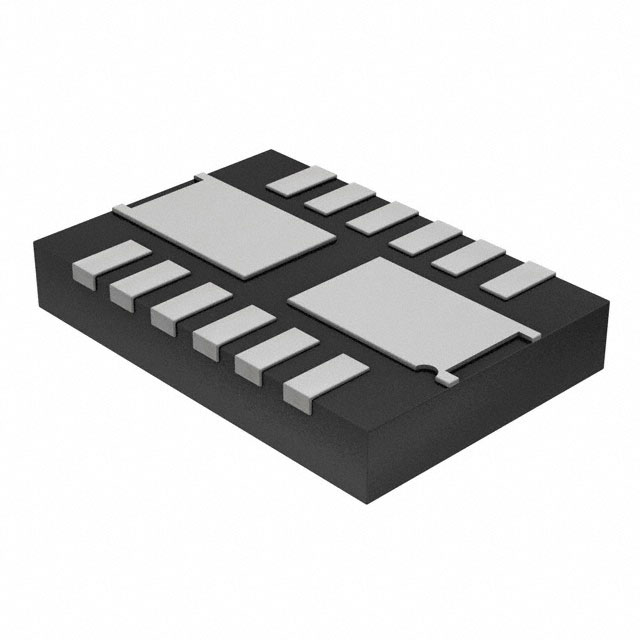
The FDMD8260L is a dual N-channel MOSFET array manufactured by onsemi, designed for surface mount applications requiring 60V drain-to-source voltage capability and 15A continuous drain current. The device is housed in a 12-PowerWDFN package measuring 3.3x5mm and operates across the industrial temperature range of -55°C to 150°C.
The FDMD8260L carries an obsolete product status. Identification of equivalent and substitute components is necessary to maintain design continuity, ensure supply chain availability, and support ongoing production requirements for applications currently utilizing this device.
Substiute Parts
Key Parameters
| Parameter | Value | Unit |
|---|---|---|
| Drain to Source Voltage (Vdss) | 60 | V |
| Current - Continuous Drain (Id) @ 25°C | 15 | A |
| Rds On (Max) @ Id, Vgs | 5.8 @ 15A, 10V | mOhm |
| Vgs(th) (Max) @ Id | 3 @ 250µA | V |
| Gate Charge (Qg) (Max) @ Vgs | 68 @ 10V | nC |
| Input Capacitance (Ciss) (Max) @ Vds | 5245 @ 30V | pF |
| Power - Max | 1 | W |
| Operating Temperature Range | -55 to 150 | °C (TJ) |
| Configuration | 2 N-Channel (Dual) | — |
| Package / Case | 12-PowerWDFN | — |
| Mounting Type | Surface Mount | — |
Substitute Part Grouping Explanation
Substitution of the FDMD8260L is determined by electrical and mechanical compatibility across the following critical parameters:
Electrical Compatibility Criteria:
- Drain to Source Voltage (Vdss): Must equal or exceed 60V
- Configuration: Must maintain 2 N-Channel (Dual) topology
- Operating Temperature Range: Must support -55°C to 150°C
- Technology: MOSFET (Metal Oxide)
Mechanical Compatibility Criteria:
- Mounting Type: Surface Mount
- Package Family: 12-Power series packages
Performance Considerations:
- Continuous drain current (Id) and on-resistance (Rds On) determine thermal and switching performance
- Gate charge (Qg) and input capacitance (Ciss) affect switching speed and gate drive requirements
- Maximum power dissipation capability influences thermal management
The substitute part NTTFD9D0N06HLTWG meets the core electrical and mechanical compatibility requirements while offering active product status and enhanced thermal performance characteristics.
Parameter Comparison
| Parameter | FDMD8260L | NTTFD9D0N06HLTWG | Unit |
|---|---|---|---|
| Manufacturer | onsemi | onsemi | — |
| Drain to Source Voltage (Vdss) | 60 | 60 | V |
| Current - Continuous Drain (Id) @ 25°C | 15 | 9 (Ta), 38 (Tc) | A |
| Rds On (Max) @ Id, Vgs | 5.8 @ 15A, 10V | 9 @ 10A, 10V | mOhm |
| Vgs(th) (Max) @ Id | 3 @ 250µA | 2 @ 50µA | V |
| Gate Charge (Qg) (Max) @ Vgs | 68 @ 10V | 13.5 @ 10V | nC |
| Input Capacitance (Ciss) (Max) @ Vds | 5245 @ 30V | 948 @ 30V | pF |
| Power - Max | 1 | 1.7 (Ta), 26 (Tc) | W |
| Operating Temperature Range | -55 to 150 | -55 to 150 | °C (TJ) |
| Configuration | 2 N-Channel (Dual) | 2 N-Channel (Dual) | — |
| Package / Case | 12-PowerWDFN | 12-PowerWQFN | — |
| Supplier Device Package | 12-Power3.3x5 | 12-WQFN (3.3x3.3) | — |
| Mounting Type | Surface Mount | Surface Mount | — |
| Product Status | Obsolete | Active | — |
| RoHS Status | ROHS3 Compliant | ROHS3 Compliant | — |
| Moisture Sensitivity Level (MSL) | 1 (Unlimited) | 1 (Unlimited) | — |
| REACH Status | REACH Unaffected | REACH Unaffected | — |
Engineering Selection Recommendations
Product Status Consideration: The FDMD8260L is classified as obsolete, which restricts long-term availability and future supply chain support. The NTTFD9D0N06HLTWG maintains active product status, ensuring continued manufacturing support and availability for new designs and production continuity.
Compliance and Certification: Both devices maintain identical regulatory compliance profiles:
- ROHS3 Compliant
- REACH Unaffected
- MSL 1 (Unlimited moisture sensitivity level)
- ECCN EAR99 classification
Electrical Compatibility: Both devices share identical Vdss (60V) and operating temperature range (-55°C to 150°C), confirming core electrical compatibility. The dual N-channel configuration is preserved in both devices.
Package Consideration: The NTTFD9D0N06HLTWG utilizes a 12-WQFN (3.3x3.3mm) package compared to the FDMD8260L's 12-Power3.3x5mm package. Both are surface mount 12-pin power packages within the onsemi PowerWDFN/PowerWQFN family. PCB layout modifications are required to accommodate the different package footprint.
Performance Characteristics: The NTTFD9D0N06HLTWG exhibits lower gate charge (13.5nC versus 68nC) and significantly reduced input capacitance (948pF versus 5245pF), resulting in faster switching characteristics and reduced gate drive power requirements. The substitute device demonstrates improved thermal performance with maximum power dissipation of 26W (Tc) compared to 1W for the original device.
Frequently Asked Questions (FAQ)
Q: Can the NTTFD9D0N06HLTWG directly replace the FDMD8260L without circuit modifications?
A: Electrical substitution is valid based on matching Vdss (60V), configuration (dual N-channel), and operating temperature range. However, package footprint differences require PCB layout modifications. The NTTFD9D0N06HLTWG's reduced gate charge and input capacitance may improve circuit performance but do not prevent substitution.
Q: What are the key differences in continuous drain current ratings?
A: The FDMD8260L specifies 15A continuous drain current at 25°C. The NTTFD9D0N06HLTWG specifies 9A at ambient temperature (Ta) and 38A at case temperature (Tc). Application-specific thermal conditions determine which rating applies. For applications operating at or near case temperature, the substitute device provides superior current handling capability.
Q: How do the on-resistance specifications compare?
A: The FDMD8260L specifies 5.8mOhm maximum at 15A and 10V gate-source voltage. The NTTFD9D0N06HLTWG specifies 9mOhm maximum at 10A and 10V gate-source voltage. The substitute device exhibits higher on-resistance at the specified test current, but improved thermal performance may offset this difference in practical applications.
Q: Are there gate drive circuit implications?
A: Yes. The NTTFD9D0N06HLTWG exhibits significantly lower gate charge (13.5nC versus 68nC) and input capacitance (948pF versus 5245pF). Existing gate drive circuits designed for the FDMD8260L will operate the substitute device with reduced power dissipation and faster switching transitions. No circuit redesign is required, but performance improvements are expected.
Q: What package considerations apply to PCB design?
A: The FDMD8260L uses a 12-Power3.3x5mm package footprint. The NTTFD9D0N06HLTWG uses a 12-WQFN (3.3x3.3mm) footprint. Both are surface mount packages within the onsemi power package family. PCB layout, trace routing, and thermal management pad design require modification to accommodate the different package dimensions and pin configuration.
Q: Are regulatory and compliance certifications identical?
A: Both devices maintain identical regulatory compliance: ROHS3 Compliant, REACH Unaffected, MSL 1 (Unlimited), and EAR99 ECCN classification. No compliance-related design changes are required for substitution.
Q: Why is product status relevant for component selection?
A: The FDMD8260L is obsolete, indicating discontinued manufacturing and restricted future availability. The NTTFD9D0N06HLTWG maintains active product status, ensuring continued supply chain support, manufacturing consistency, and availability for production quantities. Active status is preferred for new designs and long-term production requirements.
Alternative Parts

SJ6012L2TP
Littelfuse Inc.
6 Alternative Parts

JMK107BBJ476MA-RE
Taiyo Yuden
10 Alternative Parts

GMK107BBJ475MA-T
Taiyo Yuden
5 Alternative Parts
SJ6020N2ARP
Littelfuse Inc.
3 Alternative Parts
SJ6025R2ATP
Littelfuse Inc.
4 Alternative Parts

2474-05L
API Delevan Inc.
1 Alternative Parts

4590R-684K
API Delevan Inc.
1 Alternative Parts

CM6560R-334
API Delevan Inc.
1 Alternative Parts

CM6460-104
API Delevan Inc.
1 Alternative Parts

5526-12
API Delevan Inc.
1 Alternative Parts