


Request Quote
(Ships tomorrow)
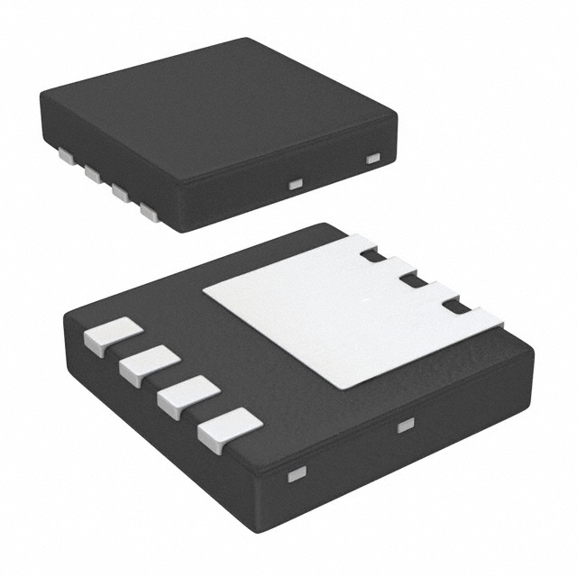
FDMC8588A N-Channel MOSFET Equivalent & Substitute Parts
Part Overview
The FDMC8588A is an N-Channel MOSFET manufactured by onsemi, part of the PowerTrench® series. This device is rated for 25 V drain-to-source voltage with continuous drain current of 16.5 A (Ta) and 40 A (Tc) in a surface mount Power33 package. The FDMC8588A is classified as obsolete product status. Identification of equivalent and substitute parts is necessary to maintain design continuity, ensure supply chain availability, and support ongoing production requirements for applications utilizing this component.
Substiute Parts
Key Parameters
| Parameter | Value | Unit |
|---|---|---|
| Manufacturer | onsemi | — |
| Series | PowerTrench® | — |
| FET Type | N-Channel | — |
| Technology | MOSFET (Metal Oxide) | — |
| Drain to Source Voltage (Vdss) | 25 | V |
| Continuous Drain Current @ 25°C (Ta) | 16.5 | A |
| Continuous Drain Current @ 25°C (Tc) | 40 | A |
| Rds On (Max) @ Id, Vgs | 5 mOhm @ 17 A, 10 V | — |
| Gate Threshold Voltage (Vgs(th)) @ Id | 1.8 | V @ 250 µA |
| Gate Charge (Qg) @ Vgs | 17 | nC @ 4.5 V |
| Input Capacitance (Ciss) @ Vds | 1720 | pF @ 13 V |
| Power Dissipation (Ta) | 2.4 | W |
| Power Dissipation (Tc) | 26 | W |
| Operating Temperature Range | −55 to 150 | °C (TJ) |
| Mounting Type | Surface Mount | — |
| Package / Case | 8-PowerTDFN | — |
| Supplier Device Package | Power33 | — |
| Product Status | Obsolete | — |
| RoHS Status | ROHS3 Compliant | — |
| REACH Status | REACH Unaffected | — |
Substitute Part Grouping Explanation
Substitution of the FDMC8588A is determined by electrical and mechanical compatibility within the N-Channel MOSFET category. The primary substitution candidate is the FDMC8651, which shares the following critical parameters:
Substitution Criteria:
- FET Type: Both devices are N-Channel MOSFETs
- Technology: Both utilize Metal Oxide MOSFET technology
- Series: Both belong to the PowerTrench® series
- Package: Both use 8-PowerTDFN package with Power33 supplier device package
- Mounting Type: Both are surface mount devices
- Operating Temperature Range: Both operate from −55°C to 150°C (TJ)
- Compliance: Both are ROHS3 Compliant and REACH Unaffected
Electrical Differences Requiring Evaluation:
The FDMC8651 operates at a higher drain-to-source voltage rating (30 V versus 25 V) and exhibits different continuous drain current specifications, on-resistance characteristics, and gate charge parameters. These differences must be evaluated against specific application requirements to determine functional equivalence.
Parameter Comparison
| Parameter | FDMC8588A | FDMC8651 | Unit |
|---|---|---|---|
| Manufacturer | onsemi | onsemi | — |
| Series | PowerTrench® | PowerTrench® | — |
| FET Type | N-Channel | N-Channel | — |
| Technology | MOSFET (Metal Oxide) | MOSFET (Metal Oxide) | — |
| Drain to Source Voltage (Vdss) | 25 | 30 | V |
| Continuous Drain Current @ 25°C (Ta) | 16.5 | 15 | A |
| Continuous Drain Current @ 25°C (Tc) | 40 | 20 | A |
| Rds On (Max) @ Id, Vgs | 5 mOhm @ 17 A, 10 V | 6.1 mOhm @ 15 A, 4.5 V | — |
| Gate Threshold Voltage (Vgs(th)) @ Id | 1.8 | 1.5 | V @ 250 µA |
| Gate Charge (Qg) @ Vgs | 17 | 27.2 | nC @ 4.5 V |
| Input Capacitance (Ciss) @ Vds | 1720 | 3365 | pF @ Vds |
| Power Dissipation (Ta) | 2.4 | 2.3 | W |
| Power Dissipation (Tc) | 26 | 41 | W |
| Operating Temperature Range | −55 to 150 | −55 to 150 | °C (TJ) |
| Mounting Type | Surface Mount | Surface Mount | — |
| Package / Case | 8-PowerTDFN | 8-PowerTDFN | — |
| Supplier Device Package | Power33 | Power33 | — |
| Product Status | Obsolete | Active | — |
| RoHS Status | ROHS3 Compliant | ROHS3 Compliant | — |
| REACH Status | REACH Unaffected | REACH Unaffected | — |
Engineering Selection Recommendations
The FDMC8651 is the designated substitute for the obsolete FDMC8588A based on product status and regulatory compliance alignment. Both devices maintain ROHS3 Compliant and REACH Unaffected certifications, ensuring regulatory continuity.
The FDMC8651 carries Active product status, providing ongoing manufacturer support and supply chain availability. This addresses the primary limitation of the FDMC8588A, which is classified as Obsolete.
Both devices share identical mechanical compatibility: 8-PowerTDFN package, Power33 supplier device package, and surface mount mounting type. PCB layout and thermal management designs developed for the FDMC8588A are directly applicable to the FDMC8651.
The FDMC8651 operates at a higher voltage rating (30 V versus 25 V), providing enhanced voltage margin in applications where the FDMC8588A operates below its maximum Vdss specification. This characteristic supports design robustness in circuits with voltage transients or supply variations.
Electrical parameter differences between the devices require circuit-level evaluation. The FDMC8651 exhibits higher gate charge (27.2 nC versus 17 nC) and input capacitance (3365 pF versus 1720 pF), which impact gate drive requirements and switching speed characteristics. Applications with stringent switching frequency or gate drive current constraints must account for these differences.
Frequently Asked Questions (FAQ)
Q: Can the FDMC8651 directly replace the FDMC8588A in existing designs?
A: Mechanical and package compatibility is direct. Electrical compatibility depends on application-specific requirements. The FDMC8651 higher voltage rating (30 V) accommodates applications designed for the FDMC8588A (25 V). However, differences in continuous drain current ratings, on-resistance, gate charge, and input capacitance require circuit analysis to confirm functional equivalence for specific applications.
Q: What are the primary electrical differences between these devices?
A: The FDMC8651 operates at 30 V Vdss compared to 25 V for the FDMC8588A. Continuous drain current specifications differ: FDMC8588A provides 16.5 A (Ta) and 40 A (Tc), while FDMC8651 provides 15 A (Ta) and 20 A (Tc). On-resistance is higher in the FDMC8651 (6.1 mOhm versus 5 mOhm). Gate charge and input capacitance are significantly higher in the FDMC8651, affecting switching characteristics and gate drive circuit design.
Q: Are there compliance or regulatory differences between these parts?
A: Both devices maintain identical compliance status: ROHS3 Compliant and REACH Unaffected. No regulatory barriers exist to substitution from a compliance perspective.
Q: What is the impact of higher gate charge in the FDMC8651?
A: Gate charge of 27.2 nC (FDMC8651) versus 17 nC (FDMC8588A) increases the charge required to switch the device. This results in higher gate drive current requirements and potentially longer switching times. Gate drive circuits must be evaluated to ensure adequate current sourcing capability at the intended switching frequency.
Q: How does the higher input capacitance of the FDMC8651 affect circuit performance?
A: Input capacitance of 3365 pF (FDMC8651) versus 1720 pF (FDMC8588A) increases the capacitive load on the gate drive circuit. This increases gate drive power dissipation and may require gate drive circuit optimization to maintain switching speed and efficiency targets.
Q: Is the FDMC8651 suitable for applications requiring the FDMC8588A continuous drain current specifications?
A: The FDMC8651 continuous drain current ratings (15 A Ta, 20 A Tc) are lower than the FDMC8588A (16.5 A Ta, 40 A Tc). Applications requiring the full current capability of the FDMC8588A must evaluate whether the FDMC8651 current ratings are sufficient for the intended load.
Q: What is the significance of the FDMC8588A being classified as Obsolete?
A: Obsolete status indicates the manufacturer has discontinued production and support. The FDMC8651 Active status ensures ongoing availability, technical support, and supply chain continuity. Substitution to the FDMC8651 is necessary for long-term design sustainability.
Q: Are the thermal characteristics equivalent between these devices?
A: Power dissipation ratings differ. FDMC8588A: 2.4 W (Ta), 26 W (Tc). FDMC8651: 2.3 W (Ta), 41 W (Tc). The FDMC8651 exhibits higher thermal dissipation at Tc, requiring thermal management evaluation in applications with significant power dissipation.
Q: Can PCB layouts designed for the FDMC8588A be reused for the FDMC8651?
A: Yes. Both devices use identical 8-PowerTDFN package and Power33 supplier device package. PCB footprints, pad layouts, and mechanical mounting are directly compatible. Thermal management design may require adjustment based on application power dissipation levels.
Alternative Parts

SJ6012L2TP
Littelfuse Inc.
6 Alternative Parts

JMK107BBJ476MA-RE
Taiyo Yuden
10 Alternative Parts

GMK107BBJ475MA-T
Taiyo Yuden
5 Alternative Parts
SJ6020N2ARP
Littelfuse Inc.
3 Alternative Parts
SJ6025R2ATP
Littelfuse Inc.
4 Alternative Parts

2474-05L
API Delevan Inc.
1 Alternative Parts

4590R-684K
API Delevan Inc.
1 Alternative Parts

CM6560R-334
API Delevan Inc.
1 Alternative Parts

CM6460-104
API Delevan Inc.
1 Alternative Parts

5526-12
API Delevan Inc.
1 Alternative Parts