


Request Quote
(Ships tomorrow)
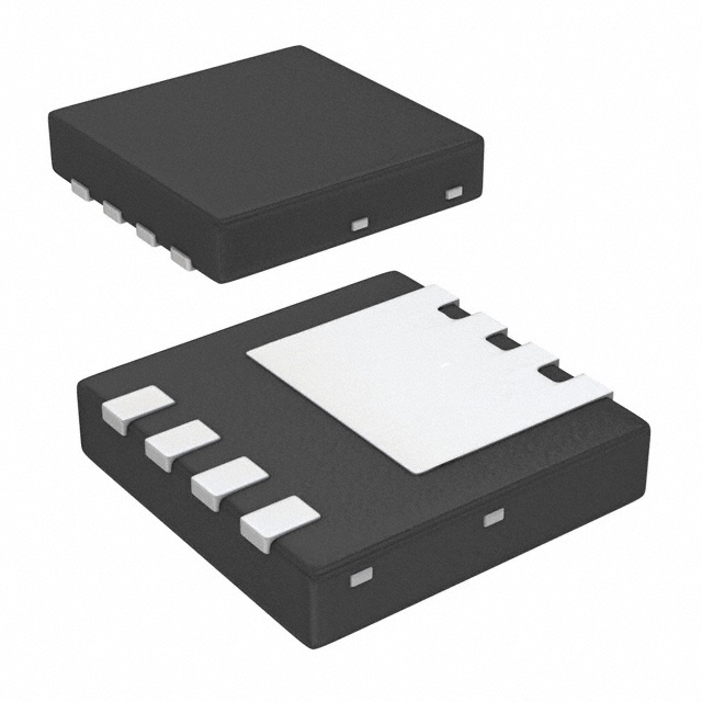
FDMC7582 N-Channel MOSFET 25V 16.7A/49A Equivalent & Substitute Parts
Part Overview
The FDMC7582 is an N-Channel MOSFET manufactured by onsemi, rated for 25V drain-to-source voltage with continuous drain current of 16.7A at Ta and 49A at Tc. This device is housed in an 8-PowerTDFN surface mount package and is part of the PowerTrench® series. The FDMC7582 is classified as obsolete, making identification of equivalent and substitute parts essential for ongoing design support and production continuity. Substitute parts must maintain electrical compatibility across voltage ratings, current handling, gate charge characteristics, and thermal performance parameters while accommodating available packaging options.
Substiute Parts
Key Parameters
| Parameter | Value | Unit |
|---|---|---|
| Drain-to-Source Voltage (Vdss) | 25 | V |
| Continuous Drain Current @ 25°C (Ta) | 16.7 | A |
| Continuous Drain Current @ 25°C (Tc) | 49 | A |
| On-Resistance (Rds On Max) @ Id, Vgs | 5 mOhm @ 16.7A, 10V | mOhm |
| Gate Threshold Voltage (Vgs(th) Max) @ Id | 2.5 | V @ 250µA |
| Gate Charge (Qg Max) @ Vgs | 28 | nC @ 10V |
| Input Capacitance (Ciss Max) @ Vds | 1795 | pF @ 13V |
| Power Dissipation (Ta) | 2.3 | W |
| Power Dissipation (Tc) | 52 | W |
| Operating Temperature Range | -55 to 150 | °C (TJ) |
| Package Type | 8-PowerTDFN | Surface Mount |
| RoHS Status | ROHS3 Compliant | - |
| Moisture Sensitivity Level | 1 (Unlimited) | - |
Substitute Part Grouping Explanation
Substitution of the FDMC7582 is determined by strict equivalence across the following electrical and mechanical parameters:
Primary Substitution Criteria:
- Drain-to-Source Voltage (Vdss): Must equal or exceed 25V
- Continuous Drain Current: Must meet or exceed 16.7A @ Ta and 49A @ Tc
- On-Resistance (Rds On): Must not exceed 5 mOhm @ specified Id and Vgs conditions
- Gate Charge (Qg): Must not exceed 28 nC @ 10V to maintain gate drive compatibility
- Input Capacitance (Ciss): Must not exceed 1795 pF @ 13V for circuit timing considerations
- Operating Temperature Range: Must support -55°C to 150°C (TJ)
- Package Type: Surface mount configuration with compatible footprint
- Compliance: RoHS3 compliant, MSL 1, REACH unaffected
Identified Substitute Parts:
- CSD16413Q5A (Texas Instruments, NexFET™ series, Active status)
- CSD16340Q3T (Texas Instruments, NexFET™ series, Active status)
Both substitute parts are active products from Texas Instruments, providing design continuity and long-term availability advantages over the obsolete FDMC7582.
Parameter Comparison
| Parameter | FDMC7582 (onsemi) | CSD16413Q5A (TI) | CSD16340Q3T (TI) | Unit |
|---|---|---|---|---|
| Manufacturer | onsemi | Texas Instruments | Texas Instruments | - |
| Product Status | Obsolete | Active | Active | - |
| FET Type | N-Channel | N-Channel | N-Channel | - |
| Vdss | 25 | 25 | 25 | V |
| Continuous Drain Current (Ta) | 16.7 | 24 | - | A |
| Continuous Drain Current (Tc) | 49 | 100 | 60 | A |
| Rds On (Max) @ Id, Vgs | 5 mOhm @ 16.7A, 10V | 3.9 mOhm @ 24A, 10V | 4.5 mOhm @ 20A, 8V | mOhm |
| Vgs(th) (Max) @ Id | 2.5 | 1.9 | 1.1 | V @ 250µA |
| Gate Charge (Qg Max) @ Vgs | 28 @ 10V | 11.7 @ 4.5V | 9.2 @ 4.5V | nC |
| Input Capacitance (Ciss Max) @ Vds | 1795 @ 13V | 1780 @ 12.5V | 1350 @ 12.5V | pF |
| Power Dissipation (Ta) | 2.3 | 3.1 | 3 | W |
| Power Dissipation (Tc) | 52 | - | - | W |
| Operating Temperature Range | -55 to 150 | -55 to 150 | -55 to 150 | °C (TJ) |
| Package Type | 8-PowerTDFN | 8-VSONP (5x6) | 8-VSON-CLIP (3.3x3.3) | - |
| RoHS Status | ROHS3 Compliant | ROHS3 Compliant | ROHS3 Compliant | - |
| Moisture Sensitivity Level | 1 (Unlimited) | 1 (Unlimited) | 1 (Unlimited) | - |
| REACH Status | REACH Unaffected | REACH Unaffected | REACH Unaffected | - |
Engineering Selection Recommendations
CSD16413Q5A (Texas Instruments NexFET™)
The CSD16413Q5A is an active product offering superior electrical performance to the obsolete FDMC7582. This device exceeds the continuous drain current requirement with 24A @ Ta and 100A @ Tc, providing design margin for thermal and electrical stress. The on-resistance of 3.9 mOhm @ 24A, 10V is lower than the FDMC7582 specification, reducing power dissipation in equivalent applications. Gate charge of 11.7 nC @ 4.5V is significantly lower, enabling faster switching and reduced gate drive power requirements. Input capacitance of 1780 pF @ 12.5V remains within acceptable limits for circuit timing. The device is supplied in 8-VSONP (5x6) packaging, which differs from the original 8-PowerTDFN footprint and requires PCB layout modification. RoHS3 compliance, MSL 1 rating, and REACH unaffected status ensure regulatory and supply chain continuity.
CSD16340Q3T (Texas Instruments NexFET™)
The CSD16340Q3T is an active product providing the highest current capability among available substitutes, with 60A @ Tc. This device delivers the lowest on-resistance at 4.5 mOhm @ 20A, 8V and the lowest gate charge at 9.2 nC @ 4.5V, optimizing for minimal switching losses and gate drive requirements. Input capacitance of 1350 pF @ 12.5V is the lowest among all options, supporting high-frequency switching applications. The device is packaged in 8-VSON-CLIP (3.3x3.3), a compact surface mount configuration that differs from the original 8-PowerTDFN footprint. Gate threshold voltage of 1.1V @ 250µA is lower than the FDMC7582, requiring verification of gate drive voltage compatibility in existing circuits. RoHS3 compliance, MSL 1 rating, and REACH unaffected status maintain regulatory alignment.
Selection Basis:
Both substitute parts are active products from Texas Instruments, eliminating obsolescence risk associated with the FDMC7582. Selection between CSD16413Q5A and CSD16340Q3T depends on specific application requirements: CSD16413Q5A offers balanced performance with moderate current capability and gate charge, while CSD16340Q3T prioritizes maximum current handling and minimal switching losses. PCB layout modification is required for either substitute due to package differences. Gate drive voltage compatibility must be evaluated for each application, as both substitutes exhibit lower gate threshold voltages than the original device.
Frequently Asked Questions (FAQ)
Q: Can the CSD16413Q5A or CSD16340Q3T be used as direct pin-for-pin replacements for the FDMC7582?
A: Both substitute parts are N-Channel MOSFETs with 8-pin surface mount packages, but they are not pin-for-pin compatible with the FDMC7582. The FDMC7582 uses an 8-PowerTDFN package, while CSD16413Q5A uses 8-VSONP (5x6) and CSD16340Q3T uses 8-VSON-CLIP (3.3x3.3). PCB layout and footprint modifications are required for either substitute.
Q: What are the key electrical differences between the FDMC7582 and its substitutes?
A: All three devices share the same 25V Vdss rating and operating temperature range (-55°C to 150°C). The primary differences are continuous drain current (FDMC7582: 16.7A Ta / 49A Tc; CSD16413Q5A: 24A Ta / 100A Tc; CSD16340Q3T: 60A Tc), on-resistance (FDMC7582: 5 mOhm; CSD16413Q5A: 3.9 mOhm; CSD16340Q3T: 4.5 mOhm), gate charge (FDMC7582: 28 nC; CSD16413Q5A: 11.7 nC; CSD16340Q3T: 9.2 nC), and input capacitance (FDMC7582: 1795 pF; CSD16413Q5A: 1780 pF; CSD16340Q3T: 1350 pF).
Q: Are the substitute parts compliant with the same regulatory standards as the FDMC7582?
A: Yes. Both CSD16413Q5A and CSD16340Q3T are RoHS3 compliant, carry MSL 1 (Unlimited) moisture sensitivity rating, and are REACH unaffected, matching the compliance profile of the FDMC7582.
Q: What is the impact of lower gate threshold voltage in the substitute parts?
A: The CSD16413Q5A has a gate threshold voltage of 1.9V @ 250µA, and the CSD16340Q3T has 1.1V @ 250µA, compared to the FDMC7582 at 2.5V @ 250µA. Lower threshold voltage means the device turns on at lower gate drive voltages. Existing gate drive circuits must be evaluated to ensure adequate voltage margin and switching performance. This is particularly important for the CSD16340Q3T due to its significantly lower threshold voltage.
Q: How does the lower gate charge of the substitute parts affect circuit design?
A: The CSD16413Q5A (11.7 nC @ 4.5V) and CSD16340Q3T (9.2 nC @ 4.5V) have substantially lower gate charge than the FDMC7582 (28 nC @ 10V). Lower gate charge reduces the energy required to switch the device and decreases gate drive power dissipation. This allows for faster switching speeds and reduced gate driver current requirements, potentially enabling use of lower-rated gate driver ICs.
Q: What packaging considerations apply when substituting these parts?
A: The FDMC7582 (8-PowerTDFN) has a different footprint than both substitutes. The CSD16413Q5A (8-VSONP, 5x6) is larger, while the CSD16340Q3T (8-VSON-CLIP, 3.3x3.3) is more compact. PCB layout, thermal management, and trace routing must be redesigned accordingly. Thermal performance may differ due to package geometry variations, requiring thermal analysis for applications with high power dissipation.
Q: Which substitute part should be selected for new designs?
A: For new designs, either CSD16413Q5A or CSD16340Q3T is appropriate, as both are active products with long-term availability. CSD16413Q5A offers balanced performance and moderate current capability. CSD16340Q3T provides maximum current handling and minimal switching losses but requires careful gate drive voltage evaluation due to its lower threshold voltage. Selection depends on specific application requirements for current, switching frequency, and thermal constraints.
Q: Are there any inventory or lead time considerations?
A: The FDMC7582 is obsolete with 19,634 pcs in stock. CSD16413Q5A has 9,253 pcs available, and CSD16340Q3T has 5,585 pcs available. Both substitutes are active products with ongoing manufacturing support, ensuring long-term availability beyond current inventory levels.
Alternative Parts

SJ6012L2TP
Littelfuse Inc.
6 Alternative Parts

JMK107BBJ476MA-RE
Taiyo Yuden
10 Alternative Parts

GMK107BBJ475MA-T
Taiyo Yuden
5 Alternative Parts
SJ6020N2ARP
Littelfuse Inc.
3 Alternative Parts
SJ6025R2ATP
Littelfuse Inc.
4 Alternative Parts

2474-05L
API Delevan Inc.
1 Alternative Parts

4590R-684K
API Delevan Inc.
1 Alternative Parts

CM6560R-334
API Delevan Inc.
1 Alternative Parts

CM6460-104
API Delevan Inc.
1 Alternative Parts

5526-12
API Delevan Inc.
1 Alternative Parts