


Request Quote
(Ships tomorrow)
FDMC6688P P-Channel MOSFET Equivalent & Substitute Parts
Part Overview
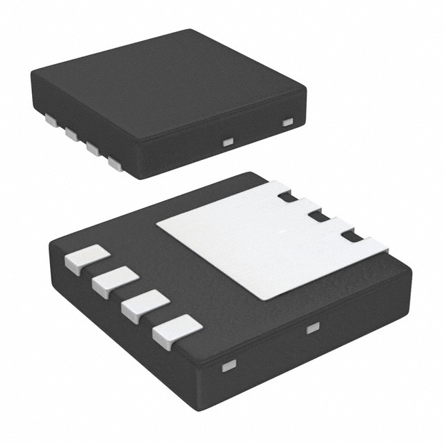
The FDMC6688P is a P-Channel enhancement mode MOSFET manufactured by onsemi, rated for 20V drain-to-source voltage with continuous drain current of 14A at Ta and 56A at Tc. This device is packaged in an 8-PQFN (3.3x3.3) surface mount configuration and is part of the PowerTrench® series. The FDMC6688P is classified as obsolete, making identification of equivalent substitute components necessary for ongoing design support, production continuity, and system maintenance applications.
Substiute Parts
Key Parameters
| Parameter | Value | Unit |
|---|---|---|
| FET Type | P-Channel | — |
| Drain to Source Voltage (Vdss) | 20 | V |
| Continuous Drain Current @ 25°C (Ta) | 14 | A |
| Continuous Drain Current @ 25°C (Tc) | 56 | A |
| Rds On (Max) @ Id, Vgs | 6.5 mOhm @ 14A, 4.5V | — |
| Gate Threshold Voltage Vgs(th) (Max) | 1 | V @ 250µA |
| Gate Charge (Qg) (Max) | 61 | nC @ 4.5V |
| Input Capacitance (Ciss) (Max) | 7435 | pF @ 10V |
| Power Dissipation (Max) (Ta) | 2.3 | W |
| Power Dissipation (Max) (Tc) | 30 | W |
| Operating Temperature Range | -55 to 150 | °C (TJ) |
| Mounting Type | Surface Mount | — |
| Package | 8-PQFN (3.3x3.3), Power33 | — |
| RoHS Status | ROHS3 Compliant | — |
| Moisture Sensitivity Level (MSL) | 1 (Unlimited) | — |
Substitute Part Grouping Explanation
Substitution of the FDMC6688P is determined by strict equivalence across the following critical parameters:
Electrical Equivalence Criteria:
- FET Type: P-Channel enhancement mode MOSFET
- Drain to Source Voltage (Vdss): 20V minimum rating
- Continuous Drain Current: Minimum 14A @ Ta and 56A @ Tc
- Gate Threshold Voltage: 1V @ 250µA maximum
- Rds On: Maximum 6.5 mOhm @ specified conditions
- Gate Charge: Maximum 61 nC @ 4.5V
- Input Capacitance: Maximum 7435 pF @ 10V
- Operating Temperature Range: -55°C to 150°C minimum
Mechanical & Compliance Equivalence Criteria:
- Mounting Type: Surface Mount
- Package Type: 8-pin DFN/PQFN variants with compatible pinout
- RoHS3 Compliance: Required
- MSL Rating: 1 (Unlimited) or equivalent
- REACH Status: Unaffected
The PJQ4411P_R2_00001 meets these substitution criteria with equivalent electrical performance and compliance certifications.
Parameter Comparison
| Parameter | FDMC6688P (onsemi) | PJQ4411P_R2_00001 (Panjit) | Compatibility |
|---|---|---|---|
| FET Type | P-Channel | P-Channel | Equivalent |
| Drain to Source Voltage (Vdss) | 20V | 20V | Equivalent |
| Continuous Drain Current @ Ta | 14A | 13A | Substitute rated lower; acceptable for applications ≤13A |
| Continuous Drain Current @ Tc | 56A | 60A | Substitute rated higher; acceptable |
| Rds On (Max) @ Id, Vgs | 6.5 mOhm @ 14A, 4.5V | 8 mOhm @ 8A, 4.5V | Substitute has higher Rds On; acceptable for lower current applications |
| Gate Threshold Voltage Vgs(th) (Max) | 1V @ 250µA | 1V @ 250µA | Equivalent |
| Gate Charge (Qg) (Max) | 61 nC @ 4.5V | 46.8 nC @ 4.5V | Substitute rated lower; acceptable |
| Input Capacitance (Ciss) (Max) | 7435 pF @ 10V | 4659 pF @ 15V | Substitute rated lower; acceptable |
| Power Dissipation (Max) @ Ta | 2.3W | 2W | Substitute rated lower; acceptable for applications ≤2W |
| Power Dissipation (Max) @ Tc | 30W | 60W | Substitute rated higher; acceptable |
| Operating Temperature Range | -55°C to 150°C (TJ) | -55°C to 150°C (TJ) | Equivalent |
| Mounting Type | Surface Mount | Surface Mount | Equivalent |
| Package | 8-PQFN (3.3x3.3), Power33 | DFN3333-8, 8-PowerVDFN | Compatible footprint; verify PCB layout compatibility |
| RoHS Status | ROHS3 Compliant | ROHS3 Compliant | Equivalent |
| MSL Rating | 1 (Unlimited) | 1 (Unlimited) | Equivalent |
| REACH Status | REACH Unaffected | REACH Unaffected | Equivalent |
Engineering Selection Recommendations
Primary Substitute: PJQ4411P_R2_00001
The PJQ4411P_R2_00001 from Panjit International Inc. is an active product classified as suitable for direct substitution in applications where the FDMC6688P is specified. Both devices are ROHS3 compliant with MSL 1 (Unlimited) ratings and REACH unaffected status, ensuring regulatory compliance across manufacturing and deployment environments.
The substitute device maintains electrical equivalence across all critical parameters including Vdss (20V), gate threshold voltage (1V @ 250µA), and operating temperature range (-55°C to 150°C). The PJQ4411P_R2_00001 is rated for 13A continuous drain current at Ta and 60A at Tc, compared to the FDMC6688P ratings of 14A and 56A respectively. This rating differential is acceptable for applications operating at or below 13A continuous current at Ta.
The substitute exhibits lower gate charge (46.8 nC vs. 61 nC) and input capacitance (4659 pF vs. 7435 pF), which provide improved switching performance characteristics. The higher Rds On specification of the substitute (8 mOhm @ 8A, 4.5V vs. 6.5 mOhm @ 14A, 4.5V) requires evaluation in applications sensitive to on-state voltage drop.
Package compatibility between the 8-PQFN (3.3x3.3) and DFN3333-8 requires PCB layout verification to confirm pinout alignment and thermal pad connectivity.
Frequently Asked Questions (FAQ)
Q: Can the PJQ4411P_R2_00001 directly replace the FDMC6688P in all applications?
A: The PJQ4411P_R2_00001 is suitable for applications operating at continuous drain currents of 13A or less at Ta. Applications requiring the full 14A rating at Ta require evaluation of the substitute's lower current rating. The substitute's lower gate charge and input capacitance may improve switching performance in some circuit topologies.
Q: What is the difference between the package designations 8-PQFN and DFN3333-8?
A: Both packages are 8-pin surface mount configurations with 3.3mm x 3.3mm footprints. The PQFN designation indicates a power quad flat no-lead package, while DFN indicates a dual flat no-lead package. Physical dimensions and thermal pad configurations are compatible, but PCB layout files must be verified for exact pinout and thermal pad connectivity.
Q: Are there compliance or regulatory differences between the FDMC6688P and PJQ4411P_R2_00001?
A: Both devices are ROHS3 compliant, carry MSL 1 (Unlimited) ratings, and are REACH unaffected. No regulatory or compliance barriers exist for substitution.
Q: How does the higher Rds On of the substitute affect circuit performance?
A: The PJQ4411P_R2_00001 exhibits 8 mOhm Rds On at 8A, 4.5V compared to the FDMC6688P at 6.5 mOhm at 14A, 4.5V. In applications operating at lower currents, this difference may be negligible. In high-current or thermally constrained applications, the increased on-state voltage drop will result in higher power dissipation. Circuit simulation or bench testing is appropriate for applications sensitive to this parameter.
Q: What is the product status of each device?
A: The FDMC6688P is classified as obsolete, necessitating substitution for new designs and ongoing production. The PJQ4411P_R2_00001 is classified as active and is available in production quantities.
Q: Are there inventory considerations for substitution?
A: The FDMC6688P has 35,827 pieces in stock. The PJQ4411P_R2_00001 has 5,726 pieces in stock. Inventory availability should be confirmed for production planning.
Alternative Parts

SJ6012L2TP
Littelfuse Inc.
6 Alternative Parts

JMK107BBJ476MA-RE
Taiyo Yuden
10 Alternative Parts

GMK107BBJ475MA-T
Taiyo Yuden
5 Alternative Parts
SJ6020N2ARP
Littelfuse Inc.
3 Alternative Parts
SJ6025R2ATP
Littelfuse Inc.
4 Alternative Parts

2474-05L
API Delevan Inc.
1 Alternative Parts

4590R-684K
API Delevan Inc.
1 Alternative Parts

CM6560R-334
API Delevan Inc.
1 Alternative Parts

CM6460-104
API Delevan Inc.
1 Alternative Parts

5526-12
API Delevan Inc.
1 Alternative Parts