


Request Quote
(Ships tomorrow)
FDMC612PZ P-Channel MOSFET Equivalent & Substitute Parts
Part Overview
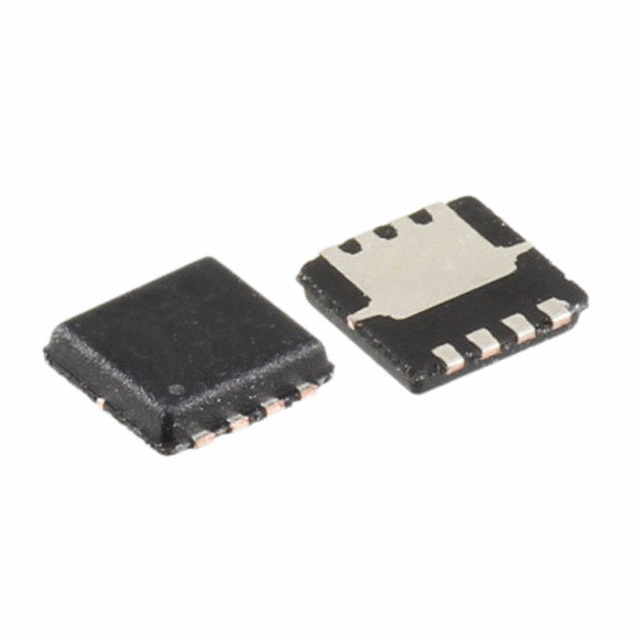
The FDMC612PZ is a P-Channel MOSFET manufactured by onsemi, rated for 20V drain-to-source voltage with 14A continuous drain current at 25°C. This device is housed in an 8-MLP (3.3x3.3) surface mount package and is part of the PowerTrench® series. The FDMC612PZ is classified as obsolete, making identification of equivalent and substitute components necessary for ongoing design support, production continuity, and system maintenance.
Substiute Parts
Key Parameters
| Parameter | Value | Unit |
|---|---|---|
| FET Type | P-Channel | — |
| Drain to Source Voltage (Vdss) | 20 | V |
| Continuous Drain Current (Id) @ 25°C | 14 | A |
| Rds On (Max) @ Id, Vgs | 8.4 mOhm @ 14A, 4.5V | — |
| Gate Threshold Voltage (Vgs(th)) @ Id | 1.5 | V @ 250µA |
| Gate Charge (Qg) @ Vgs | 74 | nC @ 4.5V |
| Maximum Gate Voltage (Vgs) | ±12 | V |
| Input Capacitance (Ciss) @ Vds | 7995 | pF @ 10V |
| Power Dissipation (Max) | 2.3 (Ta), 26 (Tc) | W |
| Operating Temperature Range | -55 to 150 | °C (TJ) |
| Mounting Type | Surface Mount | — |
| Package | 8-PowerWDFN (8-MLP 3.3x3.3) | — |
| Moisture Sensitivity Level (MSL) | 1 (Unlimited) | — |
Substitute Part Grouping Explanation
Substitution of the FDMC612PZ is determined by strict electrical and mechanical compatibility across the following critical parameters:
Electrical Compatibility Criteria:
- FET Type: P-Channel topology required
- Drain to Source Voltage (Vdss): 20V minimum rating
- Continuous Drain Current (Id): Must meet or exceed 14A at 25°C
- Gate Threshold Voltage (Vgs(th)): Compatibility with 1.5V maximum specification
- Maximum Gate Voltage (Vgs): ±12V or greater
- Operating Temperature Range: -55°C to 150°C minimum
Mechanical Compatibility Criteria:
- Mounting Type: Surface Mount only
- Package Classification: 8-pin configurations with compatible pinout and footprint dimensions
- Moisture Sensitivity Level: MSL 1 (Unlimited) preferred for handling consistency
The substitute parts listed below satisfy these criteria while maintaining functional equivalence for the FDMC612PZ in P-Channel MOSFET applications requiring 20V operation and moderate current handling.
Parameter Comparison
| Parameter | FDMC612PZ (onsemi) | CSD25402Q3A (Texas Instruments) | SIS407ADN-T1-GE3 (Vishay Siliconix) |
|---|---|---|---|
| FET Type | P-Channel | P-Channel | P-Channel |
| Vdss (V) | 20 | 20 | 20 |
| Id @ 25°C (A) | 14 (Ta) | 76 (Tc) | 18 (Tc) |
| Rds On (Max) @ Vgs 4.5V (mOhm) | 8.4 @ 14A | 8.9 @ 10A | 9 @ 15A |
| Vgs(th) (Max) @ 250µA (V) | 1.5 | 1.15 | 1 |
| Gate Charge (Qg) @ 4.5V (nC) | 74 | 9.7 | 168 |
| Vgs (Max) (V) | ±12 | ±12 | ±8 |
| Ciss @ 10V (pF) | 7995 | 1790 | 5875 |
| Power Dissipation (Ta/Tc) (W) | 2.3 / 26 | 2.8 / 69 | 3.7 / 39.1 |
| Operating Temperature (°C) | -55 to 150 | -55 to 150 | -55 to 150 |
| Mounting Type | Surface Mount | Surface Mount | Surface Mount |
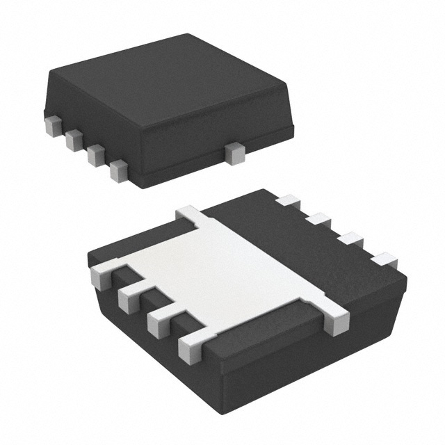
| Package | 8-PowerWDFN | 8-PowerVDFN | PowerPAK® 1212-8 |
| MSL | 1 (Unlimited) | 1 (Unlimited) | 1 (Unlimited) |
| Product Status | Obsolete | Active | Active |
Engineering Selection Recommendations
CSD25402Q3A (Texas Instruments NexFET™ Series)
The CSD25402Q3A is an active product offering superior electrical performance relative to the obsolete FDMC612PZ. This device provides 76A continuous drain current capability at case temperature, significantly exceeding the 14A requirement of the original part. The CSD25402Q3A maintains 20V Vdss rating and demonstrates lower gate charge (9.7 nC versus 74 nC), resulting in reduced switching losses and improved gate drive efficiency. The 8-PowerVDFN package is mechanically similar to the 8-PowerWDFN of the FDMC612PZ, though PCB layout verification is required due to dimensional differences. This substitute is ROHS3 compliant and carries active product status with extensive inventory availability (107,900 units in stock).
SIS407ADN-T1-GE3 (Vishay Siliconix TrenchFET® Series)
The SIS407ADN-T1-GE3 is an active product rated for 18A continuous drain current at case temperature, providing direct current capability above the 14A specification of the FDMC612PZ. This device maintains 20V Vdss rating and demonstrates lower gate threshold voltage (1V versus 1.5V), enabling more responsive gate control. The PowerPAK® 1212-8 package differs mechanically from the 8-PowerWDFN, requiring PCB footprint redesign. Gate charge is elevated at 168 nC (versus 74 nC), indicating higher switching losses. Maximum gate voltage is limited to ±8V, requiring verification against ±12V gate drive circuits. This substitute is ROHS3 compliant and carries active product status with moderate inventory availability (8,164 units in stock).
Selection Basis:
Both substitute parts satisfy the core electrical requirements (P-Channel topology, 20V Vdss, current capability ≥14A, -55°C to 150°C operating range, MSL 1). Selection between CSD25402Q3A and SIS407ADN-T1-GE3 depends on gate drive voltage constraints, switching frequency requirements, and PCB layout flexibility. The CSD25402Q3A is recommended for applications prioritizing low gate charge and high current margin. The SIS407ADN-T1-GE3 is suitable for applications with ±8V gate drive capability and moderate current requirements.
Frequently Asked Questions (FAQ)
Q: Can the CSD25402Q3A directly replace the FDMC612PZ without PCB modification?
A: The CSD25402Q3A uses an 8-PowerVDFN package while the FDMC612PZ uses 8-PowerWDFN. Although both are 8-pin surface mount packages with 3.3x3.3 mm dimensions, pinout and pad layout differences require PCB footprint verification. Direct socket replacement is not guaranteed without layout review.
Q: What is the significance of the higher gate charge (Qg) in the SIS407ADN-T1-GE3?
A: Gate charge of 168 nC (versus 74 nC in the FDMC612PZ) indicates greater capacitive loading on the gate drive circuit. This results in higher gate drive current requirements and increased switching transition times. Gate drive circuits must be verified for adequate current sourcing capability.
Q: Is the ±8V maximum gate voltage limit of the SIS407ADN-T1-GE3 compatible with ±12V gate drive circuits?
A: No. The SIS407ADN-T1-GE3 specifies ±8V maximum gate voltage. Application of ±12V gate drive voltage exceeds this rating and may cause gate oxide degradation. Gate drive circuits must be verified to operate within ±8V limits or the CSD25402Q3A (±12V rated) must be selected.
Q: Why does the CSD25402Q3A have significantly lower input capacitance (Ciss)?
A: The CSD25402Q3A demonstrates 1790 pF input capacitance versus 7995 pF in the FDMC612PZ. Lower capacitance reduces gate charge requirements and switching losses, improving overall circuit efficiency. This is a performance advantage in high-frequency switching applications.
Q: Are both substitute parts RoHS compliant?
A: Yes. Both CSD25402Q3A and SIS407ADN-T1-GE3 are ROHS3 compliant. The FDMC612PZ does not specify RoHS status. Both substitutes are REACH unaffected and carry EAR99 ECCN classification.
Q: What is the impact of the higher continuous drain current rating in the CSD25402Q3A?
A: The CSD25402Q3A is rated for 76A continuous drain current at case temperature, compared to 14A in the FDMC612PZ. This provides substantial current margin and thermal headroom. Applications operating at or near the 14A limit of the original part benefit from reduced junction temperature and extended device lifetime.
Q: Can the SIS407ADN-T1-GE3 be used in high-frequency switching applications?
A: The SIS407ADN-T1-GE3 exhibits higher gate charge (168 nC) and input capacitance (5875 pF) compared to the FDMC612PZ. These characteristics increase switching losses at high frequencies. The CSD25402Q3A is preferred for applications exceeding 100 kHz switching frequency.
Q: What inventory considerations apply to these substitutes?
A: CSD25402Q3A has extensive inventory (107,900 units in stock) with active product status, ensuring long-term availability. SIS407ADN-T1-GE3 has moderate inventory (8,164 units in stock) with active product status. Both parts are suitable for production applications requiring supply chain continuity.
Alternative Parts

SJ6012L2TP
Littelfuse Inc.
6 Alternative Parts

JMK107BBJ476MA-RE
Taiyo Yuden
10 Alternative Parts

GMK107BBJ475MA-T
Taiyo Yuden
5 Alternative Parts
SJ6020N2ARP
Littelfuse Inc.
3 Alternative Parts
SJ6025R2ATP
Littelfuse Inc.
4 Alternative Parts

2474-05L
API Delevan Inc.
1 Alternative Parts

4590R-684K
API Delevan Inc.
1 Alternative Parts

CM6560R-334
API Delevan Inc.
1 Alternative Parts

CM6460-104
API Delevan Inc.
1 Alternative Parts

5526-12
API Delevan Inc.
1 Alternative Parts