


Request Quote
(Ships tomorrow)
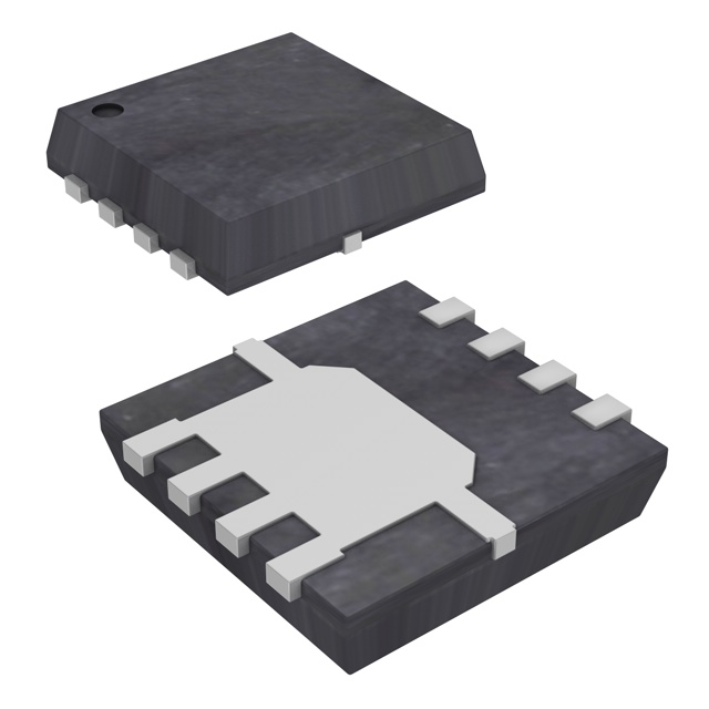
FDMC2514SDC N-Channel MOSFET Equivalent & Substitute Parts
Part Overview
The FDMC2514SDC is an N-Channel MOSFET manufactured by onsemi, rated for 25V drain-to-source voltage with continuous drain current of 24A at ambient temperature (Ta) and 40A at case temperature (Tc). This device features the Dual Cool™ 33 package technology and is designed for surface mount applications. The part is classified as obsolete, making identification of equivalent and substitute components necessary for ongoing design support, production continuity, and system maintenance.
Substiute Parts
Key Parameters
| Parameter | Value | Unit |
|---|---|---|
| Drain-to-Source Voltage (Vdss) | 25 | V |
| Continuous Drain Current @ 25°C (Ta) | 24 | A |
| Continuous Drain Current @ 25°C (Tc) | 40 | A |
| On-Resistance (Rds On Max) @ 22.5A, 10V | 3.5 | mOhm |
| Gate Threshold Voltage (Vgs(th)) @ 1mA | 3 | V |
| Gate Charge (Qg) @ 10V | 44 | nC |
| Input Capacitance (Ciss) @ 13V | 2705 | pF |
| Power Dissipation (Ta) | 3 | W |
| Power Dissipation (Tc) | 60 | W |
| Operating Temperature Range | -55 to 150 | °C |
| Package Type | 8-PowerTDFN | — |
| Mounting Type | Surface Mount | — |
Substitute Part Grouping Explanation
Substitution of the FDMC2514SDC is determined by electrical and mechanical compatibility across the following critical parameters:
Electrical Compatibility Criteria:
- Drain-to-Source Voltage (Vdss) must equal or exceed 25V
- Continuous drain current (both Ta and Tc ratings) must meet or exceed the original specification
- On-resistance (Rds On) must not exceed the original value to maintain thermal performance
- Gate threshold voltage must be compatible with existing drive circuitry
- Operating temperature range must encompass -55°C to 150°C
Mechanical Compatibility Criteria:
- Surface mount package configuration
- Pin count and footprint compatibility
- Moisture sensitivity level (MSL) rating of 1 or better
The identified substitute parts meet these criteria while offering active product status and continued availability.
Parameter Comparison
| Parameter | FDMC2514SDC | BSZ031NE2LS5ATMA1 | NTTFS4C05NTAG | Unit |
|---|---|---|---|---|
| Manufacturer | onsemi | Infineon Technologies | onsemi | — |
| Product Status | Obsolete | Active | Active | — |
| FET Type | N-Channel | N-Channel | N-Channel | — |
| Vdss | 25 | 25 | 30 | V |
| Id (Ta) | 24 | 19 | 12 | A |
| Id (Tc) | 40 | 40 | 75 | A |
| Rds On (Max) | 3.5 | 3.1 | 3.6 | mOhm |
| Vgs(th) (Max) | 3 | 2 | 2.2 | V |
| Qg (Max) | 44 | 18.3 | 31 | nC |
| Ciss (Max) | 2705 | 1230 | 1988 | pF |
| Power Dissipation (Ta) | 3 | 2.1 | 0.82 | W |
| Power Dissipation (Tc) | 60 | 30 | 33 | W |
| Operating Temperature | -55 to 150 | -55 to 150 | -55 to 150 | °C |
| Package | 8-PowerTDFN | 8-PowerTDFN | 8-PowerWDFN | — |
| Mounting Type | Surface Mount | Surface Mount | Surface Mount | — |
| RoHS Status | ROHS3 Compliant | ROHS3 Compliant | ROHS3 Compliant | — |
| MSL Rating | 1 | 1 | 1 | — |
Engineering Selection Recommendations
BSZ031NE2LS5ATMA1 (Infineon Technologies)
This substitute provides the closest electrical match to the FDMC2514SDC. Both devices share identical Vdss (25V) and Tc current rating (40A). The BSZ031NE2LS5ATMA1 features superior on-resistance (3.1 mOhm versus 3.5 mOhm) and lower gate charge (18.3 nC versus 44 nC), resulting in improved switching efficiency and reduced drive requirements. The device maintains the same 8-PowerTDFN package footprint, enabling direct board-level substitution. Active product status ensures long-term availability and supply chain continuity. RoHS3 compliance and MSL 1 rating match the original specification.
NTTFS4C05NTAG (onsemi)
This substitute offers higher voltage capability (30V Vdss) and significantly higher Tc current rating (75A), providing design margin for applications requiring increased current handling. The on-resistance (3.6 mOhm) remains within acceptable tolerance of the original specification. Gate charge is reduced (31 nC versus 44 nC), improving gate drive efficiency. The device uses an 8-PowerWDFN package, which differs from the original 8-PowerTDFN but maintains surface mount compatibility and similar thermal performance. Active product status and full compliance certifications support production deployment.
Both substitutes maintain the required operating temperature range (-55°C to 150°C), RoHS3 compliance, and MSL 1 rating. Selection between these options depends on specific application requirements regarding current capacity, voltage margin, and package footprint constraints.
Frequently Asked Questions (FAQ)
Q: Can the BSZ031NE2LS5ATMA1 be used as a direct replacement for the FDMC2514SDC?
A: The BSZ031NE2LS5ATMA1 provides electrical and mechanical compatibility for most applications. Both devices share the same Vdss (25V), Tc current rating (40A), and 8-PowerTDFN package footprint. The BSZ031NE2LS5ATMA1 offers improved performance characteristics with lower on-resistance and gate charge. Verification of gate drive voltage compatibility and thermal management is required for specific circuit implementations.
Q: What are the key differences between the two substitute parts?
A: The BSZ031NE2LS5ATMA1 matches the original voltage and case temperature current rating exactly, with superior on-resistance and lower gate charge. The NTTFS4C05NTAG provides higher voltage capability (30V) and significantly higher case temperature current rating (75A), offering greater design margin but using a different package variant (8-PowerWDFN versus 8-PowerTDFN). Both maintain identical operating temperature ranges and compliance certifications.
Q: Are there package compatibility concerns when substituting the NTTFS4C05NTAG?
A: The NTTFS4C05NTAG uses an 8-PowerWDFN (3.3x3.3) package instead of the original 8-PowerTDFN. While both are surface mount 8-pin packages, the physical dimensions and thermal pad configuration differ. PCB layout modifications may be required to accommodate the different package geometry. Thermal performance characteristics remain comparable between the two packages.
Q: Do all substitute parts maintain the same compliance certifications?
A: Yes. Both the BSZ031NE2LS5ATMA1 and NTTFS4C05NTAG are RoHS3 compliant, REACH unaffected, and carry MSL 1 (unlimited) moisture sensitivity ratings, matching the original FDMC2514SDC specifications. Both are classified under ECCN EAR99 and HTSUS 8541.29.0095.
Q: What is the impact of lower gate charge on circuit design?
A: Both substitute parts feature reduced gate charge compared to the FDMC2514SDC (18.3 nC and 31 nC versus 44 nC). Lower gate charge reduces the energy required to switch the device and decreases switching losses. Existing gate drive circuits designed for the original part will operate with improved efficiency margins. No circuit modifications are required to accommodate lower gate charge specifications.
Q: How do the on-resistance values affect thermal performance?
A: The BSZ031NE2LS5ATMA1 (3.1 mOhm) provides lower on-resistance than the original (3.5 mOhm), reducing conduction losses and improving thermal efficiency. The NTTFS4C05NTAG (3.6 mOhm) is marginally higher but remains within acceptable tolerance. In high-current applications, the lower on-resistance of the BSZ031NE2LS5ATMA1 may provide thermal advantages. Both devices maintain the same maximum power dissipation ratings at case temperature (30W and 33W respectively, compared to 60W for the original).
Q: Is the higher Vdss rating of the NTTFS4C05NTAG beneficial?
A: The 30V Vdss rating of the NTTFS4C05NTAG provides additional voltage margin compared to the 25V original specification. This higher rating offers protection against voltage transients and overshoot conditions. However, applications designed for 25V operation do not require this additional margin. Selection should be based on actual circuit voltage requirements and transient protection needs.
Alternative Parts

SJ6012L2TP
Littelfuse Inc.
6 Alternative Parts

JMK107BBJ476MA-RE
Taiyo Yuden
10 Alternative Parts

GMK107BBJ475MA-T
Taiyo Yuden
5 Alternative Parts
SJ6020N2ARP
Littelfuse Inc.
3 Alternative Parts
SJ6025R2ATP
Littelfuse Inc.
4 Alternative Parts

2474-05L
API Delevan Inc.
1 Alternative Parts

4590R-684K
API Delevan Inc.
1 Alternative Parts

CM6560R-334
API Delevan Inc.
1 Alternative Parts

CM6460-104
API Delevan Inc.
1 Alternative Parts

5526-12
API Delevan Inc.
1 Alternative Parts