


Request Quote
(Ships tomorrow)
FDMA908PZ P-Channel MOSFET Equivalent & Substitute Parts
Part Overview
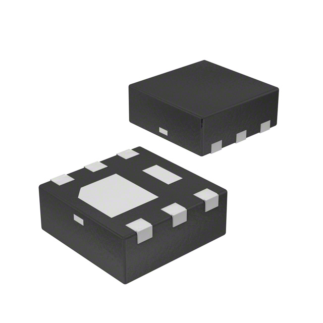
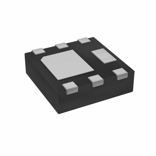
The FDMA908PZ is a P-Channel MOSFET manufactured by onsemi, rated for 12V drain-to-source voltage with 12A continuous drain current. The device is housed in a 6-MicroFET (2x2) surface mount package and features the PowerTrench® series technology. This part is designated as Last Time Buy, indicating end-of-life status. Identifying equivalent and substitute parts is necessary to ensure design continuity and maintain supply chain reliability for applications requiring P-Channel MOSFET functionality within the specified electrical and mechanical parameters.
Substiute Parts
Key Parameters
| Parameter | Value | Unit |
|---|---|---|
| FET Type | P-Channel | — |
| Drain to Source Voltage (Vdss) | 12 | V |
| Current - Continuous Drain (Id) @ 25°C | 12 | A |
| Rds On (Max) @ Id, Vgs | 12.5 | mOhm @ 12A, 4.5V |
| Vgs(th) (Max) @ Id | 1 | V @ 250µA |
| Gate Charge (Qg) (Max) @ Vgs | 34 | nC @ 4.5V |
| Power Dissipation (Max) | 2.4 | W |
| Operating Temperature Range | -55 to 150 | °C (TJ) |
| Mounting Type | Surface Mount | — |
| Package / Case | 6-WDFN Exposed Pad | — |
| RoHS Status | ROHS3 Compliant | — |
| Moisture Sensitivity Level (MSL) | 1 (Unlimited) | — |
Substitute Part Grouping Explanation
Substitution of the FDMA908PZ is determined by the following critical electrical and mechanical parameters:
Primary Substitution Criteria:
- FET Type: P-Channel topology
- Drain to Source Voltage (Vdss): 12V minimum rating
- Continuous Drain Current (Id): Minimum 12A at 25°C
- On-State Resistance (Rds On): Performance at specified gate voltage
- Gate Threshold Voltage (Vgs(th)): Compatibility with drive circuits
- Operating Temperature Range: -55°C to 150°C (TJ)
- Surface Mount Packaging: 6-pin configurations with exposed pad
- Compliance: ROHS3 and REACH requirements
The substitute parts listed below meet or exceed the FDMA908PZ electrical specifications while maintaining surface mount compatibility. Variations in package footprint (6-WDFN versus 6-UDFN) and power dissipation ratings are noted for design consideration.
Parameter Comparison
| Parameter | FDMA908PZ (onsemi) | DMP1022UFDF-13 (Diodes Inc.) | DMP1022UFDF-7 (Diodes Inc.) | SSM6J505NU,LF (Toshiba) |
|---|---|---|---|---|
| FET Type | P-Channel | P-Channel | P-Channel | P-Channel |
| Vdss (V) | 12 | 12 | 12 | 12 |
| Id @ 25°C (A) | 12 | 9.5 | 9.5 | 12 |
| Rds On (Max) @ 4.5V (mOhm) | 12.5 @ 12A | 14.8 @ 4A | 15.3 @ 4A | 12 @ 4A |
| Vgs(th) (Max) @ 250µA (V) | 1 | 0.8 | 0.8 | 1 |
| Gate Charge (Qg) @ 4.5V (nC) | 34 | 48.3 | 48.3 | 37.6 |
| Power Dissipation (Max) (W) | 2.4 | 0.73 | 0.73 | 1.25 |
| Operating Temperature (°C) | -55 to 150 | -55 to 150 | -55 to 150 | -55 to 150 |
| Package | 6-WDFN Exposed Pad | 6-UDFN Exposed Pad | 6-UDFN Exposed Pad | 6-WDFN Exposed Pad |
| RoHS Status | ROHS3 Compliant | ROHS3 Compliant | ROHS3 Compliant | ROHS3 Compliant |
| MSL | 1 (Unlimited) | 1 (Unlimited) | 1 (Unlimited) | 1 (Unlimited) |
Engineering Selection Recommendations
FDMA908PZ (onsemi) — Primary Part
- Product Status: Last Time Buy
- Recommended for: Existing designs with established supply chains; applications where PowerTrench® technology is specified
- Compliance: ROHS3 Compliant, REACH Unaffected
SSM6J505NU,LF (Toshiba) — Preferred Substitute
- Product Status: Active
- Electrical Match: Matches FDMA908PZ in continuous drain current (12A) and on-state resistance (12 mOhm @ 4A, 4.5V)
- Package Compatibility: 6-WDFN Exposed Pad (identical to FDMA908PZ)
- Compliance: ROHS3 Compliant, REACH Unaffected
- Consideration: Maximum Vgs is ±6V (versus ±8V for FDMA908PZ); verify gate drive circuit compatibility
DMP1022UFDF-13 and DMP1022UFDF-7 (Diodes Incorporated) — Secondary Substitutes
- Product Status: Active
- Electrical Differences: Continuous drain current rated at 9.5A (below FDMA908PZ 12A specification); higher on-state resistance (14.8–15.3 mOhm @ 4A, 4.5V)
- Package Difference: 6-UDFN Exposed Pad (footprint variation from FDMA908PZ 6-WDFN)
- Compliance: ROHS3 Compliant, REACH Unaffected
- Application Suitability: Appropriate for designs with reduced current requirements or where PCB layout accommodates UDFN footprint
Frequently Asked Questions (FAQ)
Q: Can DMP1022UFDF-13 or DMP1022UFDF-7 directly replace FDMA908PZ in all applications?
A: No. The DMP1022 series is rated for 9.5A continuous drain current, which is below the FDMA908PZ specification of 12A. These parts are suitable only for applications where the actual operating current does not exceed 9.5A. Additionally, the 6-UDFN package footprint differs from the FDMA908PZ 6-WDFN package, requiring PCB layout modification.
Q: Is SSM6J505NU,LF a direct pin-compatible replacement?
A: SSM6J505NU,LF shares the same 6-WDFN Exposed Pad package as FDMA908PZ and matches the 12A continuous drain current specification. However, the maximum gate-source voltage (Vgs) is ±6V for the Toshiba part versus ±8V for the onsemi part. Verify that the gate drive circuit operates within the ±6V limit before implementation.
Q: What are the key differences in on-state resistance between these parts?
A: FDMA908PZ and SSM6J505NU,LF both specify 12 mOhm maximum on-state resistance at 4.5V gate voltage (measured at different drain currents). The DMP1022 series specifies 14.8–15.3 mOhm, representing approximately 20% higher resistance. This difference affects power dissipation and thermal performance in high-current applications.
Q: Are all substitute parts RoHS3 compliant?
A: Yes. FDMA908PZ, DMP1022UFDF-13, DMP1022UFDF-7, and SSM6J505NU,LF are all ROHS3 Compliant with MSL 1 (Unlimited) moisture sensitivity rating.
Q: What is the significance of the FDMA908PZ Last Time Buy status?
A: Last Time Buy designation indicates that onsemi will discontinue production of this part. Existing inventory is available, but future availability is not guaranteed. Designs should transition to active-status alternatives such as SSM6J505NU,LF to ensure long-term supply chain continuity.
Q: How do gate charge specifications affect circuit design?
A: Gate charge (Qg) determines the energy required to switch the MOSFET. FDMA908PZ specifies 34 nC @ 4.5V, while DMP1022 series specifies 48.3 nC and SSM6J505NU,LF specifies 37.6 nC. Higher gate charge requires greater drive current or longer switching times. Verify that the gate driver circuit can supply sufficient charge within the required switching frequency.
Q: Can package footprint differences be accommodated in existing designs?
A: Package footprint differences between 6-WDFN (FDMA908PZ, SSM6J505NU,LF) and 6-UDFN (DMP1022 series) require PCB layout modification. Footprint compatibility must be verified with the PCB design tool before component selection. Pin assignments and exposed pad thermal characteristics should be confirmed against the respective datasheets.
Alternative Parts

SJ6012L2TP
Littelfuse Inc.
6 Alternative Parts

JMK107BBJ476MA-RE
Taiyo Yuden
10 Alternative Parts

GMK107BBJ475MA-T
Taiyo Yuden
5 Alternative Parts
SJ6020N2ARP
Littelfuse Inc.
3 Alternative Parts
SJ6025R2ATP
Littelfuse Inc.
4 Alternative Parts

2474-05L
API Delevan Inc.
1 Alternative Parts

4590R-684K
API Delevan Inc.
1 Alternative Parts

CM6560R-334
API Delevan Inc.
1 Alternative Parts

CM6460-104
API Delevan Inc.
1 Alternative Parts

5526-12
API Delevan Inc.
1 Alternative Parts