


Request Quote
(Ships tomorrow)
FDM6296 Equivalent & Substitute Parts
Part Overview
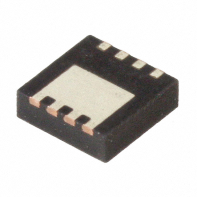
The FDM6296 is an N-Channel MOSFET manufactured by onsemi, rated for 30V drain-to-source voltage with 11.5A continuous drain current at 25°C. The device is housed in an 8-Power33 (3x3) surface mount package and is part of the PowerTrench® series. The FDM6296 is classified as obsolete, making identification of equivalent and substitute parts essential for ongoing design support and production continuity. Substitute parts must maintain electrical compatibility within the specified parameter ranges while accommodating the transition from obsolete to active product status.
Substiute Parts
Key Parameters
| Parameter | Value | Unit |
|---|---|---|
| Drain-to-Source Voltage (Vdss) | 30 | V |
| Continuous Drain Current @ 25°C (Id) | 11.5 | A (Ta) |
| On-Resistance @ 11.5A, 10V (Rds On Max) | 10.5 | mOhm |
| Gate Threshold Voltage @ 250µA (Vgs(th) Max) | 3 | V |
| Gate Charge @ 5V (Qg Max) | 17 | nC |
| Input Capacitance @ 15V (Ciss Max) | 2005 | pF |
| Power Dissipation (Ta) | 2.1 | W |
| Operating Temperature Range | -55 to 150 | °C (TJ) |
| Mounting Type | Surface Mount | |
| Package | 8-Power33 (3x3) |
Substitute Part Grouping Explanation
Substitute parts for the FDM6296 are selected based on the following electrical and mechanical criteria:
Primary Substitution Criteria:
- Drain-to-Source Voltage (Vdss) equal to or greater than 30V
- Continuous Drain Current (Id) at 25°C equal to or greater than 11.5A
- On-Resistance (Rds On) at rated current and gate voltage compatible with circuit requirements
- Gate Threshold Voltage (Vgs(th)) within acceptable switching characteristics
- Operating temperature range spanning -55°C to 150°C
- Surface mount packaging with compatible footprint dimensions
- N-Channel MOSFET technology (Metal Oxide)
Secondary Considerations:
- Product status (active vs. obsolete)
- Compliance certifications (RoHS, REACH)
- Moisture sensitivity level
- Gate charge and input capacitance characteristics for switching performance
The two substitute parts listed below meet the minimum electrical requirements for direct substitution while offering improved or equivalent performance characteristics.
Parameter Comparison
| Parameter | FDM6296 | FDMC7692 | CSD16411Q3 | Unit |
|---|---|---|---|---|
| Manufacturer | onsemi | onsemi | Texas Instruments | |
| Product Status | Obsolete | Active | Active | |
| FET Type | N-Channel | N-Channel | N-Channel | |
| Technology | MOSFET (Metal Oxide) | MOSFET (Metal Oxide) | MOSFET (Metal Oxide) | |
| Vdss | 30 | 30 | 25 | V |
| Id @ 25°C (Ta) | 11.5 | 13.3 | 14 | A |
| Rds On Max @ Id, 10V | 10.5 @ 11.5A | 8.5 @ 13.3A | 10 @ 10A | mOhm |
| Vgs(th) Max @ 250µA | 3 | 3 | 2.3 | V |
| Qg Max | 17 @ 5V | 29 @ 10V | 3.8 @ 4.5V | nC |
| Ciss Max @ Vds | 2005 @ 15V | 1680 @ 15V | 570 @ 12.5V | pF |
| Power Dissipation (Ta) | 2.1 | 2.3 | 2.7 | W |
| Operating Temperature | -55 to 150 | -55 to 150 | -55 to 150 | °C (TJ) |
| Mounting Type | Surface Mount | Surface Mount | Surface Mount | |
| Package / Case | 8-PowerVDFN | 8-PowerWDFN | 8-PowerTDFN | |
| Supplier Device Package | 8-Power33 (3x3) | 8-MLP (3.3x3.3) | 8-VSON-CLIP (3.3x3.3) | |
| RoHS Status | Not specified | ROHS3 Compliant | ROHS3 Compliant | |
| REACH Status | REACH Unaffected | REACH Unaffected | REACH Unaffected | |
| Moisture Sensitivity Level | 1 (Unlimited) | 1 (Unlimited) | 1 (Unlimited) |
Engineering Selection Recommendations
FDMC7692 (onsemi): The FDMC7692 is the primary substitute for the FDM6296. Both devices are manufactured by onsemi and share the PowerTrench® series designation. The FDMC7692 maintains the 30V Vdss rating and exceeds the continuous drain current requirement with 13.3A at 25°C (Ta). The on-resistance is improved at 8.5mOhm compared to the FDM6296's 10.5mOhm. The FDMC7692 is active product status, ensuring long-term availability and supply chain continuity. The device is ROHS3 compliant and carries identical REACH unaffected status. Package dimensions are comparable (8-MLP 3.3x3.3 vs. 8-Power33 3x3), though PCB layout verification is required due to different package designations (8-PowerWDFN vs. 8-PowerVDFN). Gate charge is higher at 29nC, which may affect switching speed in high-frequency applications.
CSD16411Q3 (Texas Instruments): The CSD16411Q3 is a secondary substitute manufactured by Texas Instruments under the NexFET™ series. This device has a lower Vdss rating of 25V, which is below the FDM6296's 30V specification. The CSD16411Q3 exceeds current requirements with 14A at 25°C (Ta) and offers superior on-resistance at 10mOhm. Gate charge is significantly lower at 3.8nC, providing faster switching characteristics. The device is ROHS3 compliant with identical REACH unaffected status. The 8-VSON-CLIP package (3.3x3.3) differs from the original 8-Power33 package, requiring PCB footprint redesign. The reduced Vdss rating limits this substitute to applications where the 25V maximum voltage is acceptable.
Selection Basis:
- FDMC7692 is recommended for direct replacement where 30V Vdss is required and supply chain continuity is prioritized
- CSD16411Q3 is suitable only for applications with maximum operating voltages of 25V or lower
- Both substitutes are active products with full compliance certifications
- Package footprint changes require PCB layout verification for either substitute
Frequently Asked Questions (FAQ)
Q: Can the FDMC7692 be used as a direct drop-in replacement for the FDM6296?
A: The FDMC7692 is electrically compatible and meets all minimum performance requirements. However, the package designation differs (8-PowerWDFN vs. 8-PowerVDFN), and physical dimensions vary slightly (8-MLP 3.3x3.3 vs. 8-Power33 3x3). PCB footprint verification is required before implementation.
Q: Why is the CSD16411Q3 listed as a substitute if it has a lower Vdss rating?
A: The CSD16411Q3 meets substitution criteria for applications where the circuit maximum voltage does not exceed 25V. The lower Vdss rating restricts its use to specific design scenarios. For applications requiring the full 30V rating, the FDMC7692 is the appropriate choice.
Q: What are the key differences in switching characteristics between these devices?
A: Gate charge (Qg) and input capacitance (Ciss) differ significantly. The FDM6296 has 17nC gate charge at 5V and 2005pF input capacitance. The FDMC7692 has 29nC at 10V and 1680pF, while the CSD16411Q3 has 3.8nC at 4.5V and 570pF. Lower gate charge enables faster switching but may require different gate drive circuit design.
Q: Are there any compliance or regulatory differences between the three devices?
A: The FDM6296 does not specify RoHS status. Both FDMC7692 and CSD16411Q3 are ROHS3 compliant. All three devices have REACH unaffected status and MSL 1 (Unlimited) moisture sensitivity. For applications requiring RoHS compliance, either substitute is acceptable.
Q: What is the impact of different package types on circuit design?
A: Package differences (8-PowerVDFN, 8-PowerWDFN, 8-PowerTDFN) require PCB layout redesign. Pin assignments, thermal pad dimensions, and trace routing may differ. Thermal performance characteristics also vary due to package construction differences. Consult device datasheets for specific package dimensions and thermal specifications before PCB redesign.
Q: Can the FDM6296 be sourced as an active product?
A: No. The FDM6296 is classified as obsolete. The FDMC7692 and CSD16411Q3 are both active products with confirmed inventory availability, ensuring long-term supply chain support.
Q: What is the maximum continuous drain current for each device at 25°C?
A: FDM6296: 11.5A (Ta). FDMC7692: 13.3A (Ta). CSD16411Q3: 14A (Ta). All devices exceed the original specification, providing design margin.
Q: Are there temperature derating considerations for these devices?
A: All three devices operate across -55°C to 150°C (TJ). The FDMC7692 and CSD16411Q3 provide additional thermal performance data at case temperature (Tc), enabling more precise thermal calculations for high-power applications. Refer to device datasheets for derating curves.
Alternative Parts

SJ6012L2TP
Littelfuse Inc.
6 Alternative Parts

JMK107BBJ476MA-RE
Taiyo Yuden
10 Alternative Parts

GMK107BBJ475MA-T
Taiyo Yuden
5 Alternative Parts
SJ6020N2ARP
Littelfuse Inc.
3 Alternative Parts
SJ6025R2ATP
Littelfuse Inc.
4 Alternative Parts

2474-05L
API Delevan Inc.
1 Alternative Parts

4590R-684K
API Delevan Inc.
1 Alternative Parts

CM6560R-334
API Delevan Inc.
1 Alternative Parts

CM6460-104
API Delevan Inc.
1 Alternative Parts

5526-12
API Delevan Inc.
1 Alternative Parts