


Request Quote
(Ships tomorrow)
FDJ1032C Equivalent & Substitute Parts
Part Overview
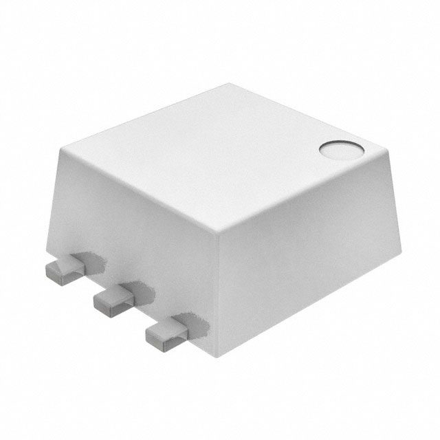
The FDJ1032C is an obsolete N and P-Channel MOSFET array manufactured by onsemi, rated for 20V drain-to-source voltage with continuous drain currents of 3.2A and 2.8A. The device features logic level gate operation and is packaged in the SC-75-6 FLMP surface mount configuration. Due to its obsolete product status, identifying functionally equivalent substitute components is necessary for ongoing design support, production continuity, and system maintenance applications.
Substiute Parts
Key Parameters
| Parameter | FDJ1032C Value |
|---|---|
| Drain to Source Voltage (Vdss) | 20V |
| Current - Continuous Drain (Id) @ 25°C | 3.2A, 2.8A |
| Rds On (Max) @ Id, Vgs | 90mOhm @ 3.2A, 4.5V |
| Vgs(th) (Max) @ Id | 1.5V @ 250µA |
| Gate Charge (Qg) (Max) @ Vgs | 3nC @ 4.5V |
| Input Capacitance (Ciss) (Max) @ Vds | 200pF @ 10V |
| Power - Max | 900mW |
| Operating Temperature | -55°C ~ 150°C (TJ) |
| Configuration | N and P-Channel |
| FET Feature | Logic Level Gate |
| Mounting Type | Surface Mount |
| Package / Case | SC-75-6 FLMP |
| Series | PowerTrench® |
| Technology | MOSFET (Metal Oxide) |
Substitute Part Grouping Explanation
Substitute components for the FDJ1032C are identified based on electrical parameter compatibility within the allowed operating ranges for this MOSFET category. The primary substitution criteria are:
Electrical Compatibility Parameters:
- Drain to Source Voltage (Vdss) rating of 20V or greater
- Continuous drain current capability meeting or exceeding 3.2A at 25°C
- On-state resistance (Rds On) at specified gate voltage and current
- Gate threshold voltage (Vgs(th)) within logic level specifications
- Gate charge and input capacitance characteristics
- Maximum power dissipation rating
- Operating temperature range encompassing -55°C to 150°C
Functional Requirements:
- N and P-Channel configuration
- Logic level gate operation
- Surface mount technology
- PowerTrench® series technology
The FDME1034CZT meets these substitution criteria through equivalent voltage ratings, enhanced current handling, improved on-state resistance characteristics, and active product status with full compliance certifications.
Parameter Comparison
| Parameter | FDJ1032C | FDME1034CZT | Compatibility Notes |
|---|---|---|---|
| Drain to Source Voltage (Vdss) | 20V | 20V | Equivalent |
| Current - Continuous Drain (Id) @ 25°C | 3.2A, 2.8A | 3.8A, 2.6A | FDME1034CZT provides higher N-channel current |
| Rds On (Max) @ Id, Vgs | 90mOhm @ 3.2A, 4.5V | 66mOhm @ 3.4A, 4.5V | FDME1034CZT offers improved on-state resistance |
| Vgs(th) (Max) @ Id | 1.5V @ 250µA | 1V @ 250µA | FDME1034CZT has lower threshold voltage |
| Gate Charge (Qg) (Max) @ Vgs | 3nC @ 4.5V | 4.2nC @ 4.5V | FDME1034CZT has slightly higher gate charge |
| Input Capacitance (Ciss) (Max) @ Vds | 200pF @ 10V | 300pF @ 10V | FDME1034CZT has higher input capacitance |
| Power - Max | 900mW | 600mW | FDME1034CZT has lower maximum power rating |
| Operating Temperature | -55°C ~ 150°C (TJ) | -55°C ~ 150°C (TJ) | Equivalent |
| Configuration | N and P-Channel | N and P-Channel | Equivalent |
| FET Feature | Logic Level Gate | Logic Level Gate | Equivalent |
| Mounting Type | Surface Mount | Surface Mount | Equivalent |
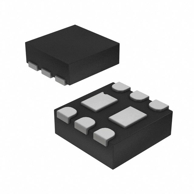
| Package / Case | SC-75-6 FLMP | 6-UFDFN Exposed Pad | Different package form factors |
| Series | PowerTrench® | PowerTrench® | Equivalent |
| Technology | MOSFET (Metal Oxide) | MOSFET (Metal Oxide) | Equivalent |
| Product Status | Obsolete | Active | FDME1034CZT is actively manufactured |
| RoHS Status | Not specified | ROHS3 Compliant | FDME1034CZT meets RoHS3 requirements |
Engineering Selection Recommendations
The FDME1034CZT serves as a functional substitute for the obsolete FDJ1032C based on the following engineering criteria:
Electrical Performance: The FDME1034CZT maintains the 20V Vdss rating and provides enhanced continuous drain current capability (3.8A N-channel versus 3.2A). The improved on-state resistance (66mOhm versus 90mOhm) results in lower power dissipation during switching operations. Both devices operate across the identical temperature range of -55°C to 150°C.
Product Status and Compliance: The FDME1034CZT is an active product with full manufacturing support, whereas the FDJ1032C is obsolete. The FDME1034CZT carries ROHS3 compliance certification, ensuring alignment with current environmental and regulatory standards. Both devices maintain REACH Unaffected status and EAR99 export classification.
Package Consideration: The primary design change involves package form factor transition from SC-75-6 FLMP to 6-UFDFN Exposed Pad (1.6x1.6mm). This transition requires PCB layout modification and thermal management evaluation, as the smaller footprint may affect heat dissipation characteristics.
Application Suitability: The FDME1034CZT is suitable for applications where the FDJ1032C was previously specified, provided that the package transition is accommodated in the design. The lower gate threshold voltage and improved on-state resistance characteristics may provide performance benefits in logic-level gate drive applications.
Frequently Asked Questions (FAQ)
Q: Can the FDME1034CZT directly replace the FDJ1032C without PCB modifications?
A: No. While the electrical parameters are compatible, the package form factors differ significantly. The FDJ1032C uses SC-75-6 FLMP packaging, while the FDME1034CZT uses 6-UFDFN Exposed Pad (1.6x1.6mm). PCB layout redesign is required to accommodate the different footprint and pin configuration.
Q: What are the key electrical advantages of the FDME1034CZT over the FDJ1032C?
A: The FDME1034CZT provides three primary electrical improvements: higher continuous drain current (3.8A versus 3.2A for the N-channel), lower on-state resistance (66mOhm versus 90mOhm), and lower gate threshold voltage (1V versus 1.5V). These characteristics result in reduced power dissipation and improved switching performance in logic-level gate drive circuits.
Q: Are there any electrical parameters where the FDJ1032C outperforms the FDME1034CZT?
A: The FDJ1032C has a higher maximum power dissipation rating (900mW versus 600mW) and lower input capacitance (200pF versus 300pF). Applications requiring maximum power handling or minimal gate drive capacitance may need to evaluate these differences against the performance benefits of the substitute.
Q: What is the significance of the different maximum power ratings?
A: The FDJ1032C is rated for 900mW maximum power dissipation, while the FDME1034CZT is rated for 600mW. However, the FDME1034CZT's lower on-state resistance typically results in lower actual power dissipation during normal operation. Applications operating near maximum power limits require thermal analysis to confirm the substitute is suitable.
Q: Does the FDME1034CZT meet current regulatory requirements?
A: Yes. The FDME1034CZT is ROHS3 compliant and maintains REACH Unaffected status, meeting current environmental and regulatory standards. The FDJ1032C's compliance status is not fully specified in the available documentation.
Q: How does the package size difference affect thermal performance?
A: The FDME1034CZT's 6-UFDFN package (1.6x1.6mm) is significantly smaller than the SC-75-6 FLMP package. Thermal performance depends on PCB copper area, via placement, and thermal management design. Applications with high power dissipation require detailed thermal analysis to ensure adequate heat dissipation with the smaller package.
Q: Are both devices from the same manufacturer?
A: Yes. Both the FDJ1032C and FDME1034CZT are manufactured by onsemi and are part of the PowerTrench® MOSFET series, ensuring consistent design philosophy and manufacturing quality standards.
Q: What is the impact of higher gate charge on circuit design?
A: The FDME1034CZT has slightly higher gate charge (4.2nC versus 3nC), requiring marginally more gate drive current and energy. This difference is typically negligible in most applications but may require evaluation in high-frequency switching circuits with limited gate drive capability.
Alternative Parts

SJ6012L2TP
Littelfuse Inc.
6 Alternative Parts

JMK107BBJ476MA-RE
Taiyo Yuden
10 Alternative Parts

GMK107BBJ475MA-T
Taiyo Yuden
5 Alternative Parts
SJ6020N2ARP
Littelfuse Inc.
3 Alternative Parts
SJ6025R2ATP
Littelfuse Inc.
4 Alternative Parts

2474-05L
API Delevan Inc.
1 Alternative Parts

4590R-684K
API Delevan Inc.
1 Alternative Parts

CM6560R-334
API Delevan Inc.
1 Alternative Parts

CM6460-104
API Delevan Inc.
1 Alternative Parts

5526-12
API Delevan Inc.
1 Alternative Parts