


Request Quote
(Ships tomorrow)
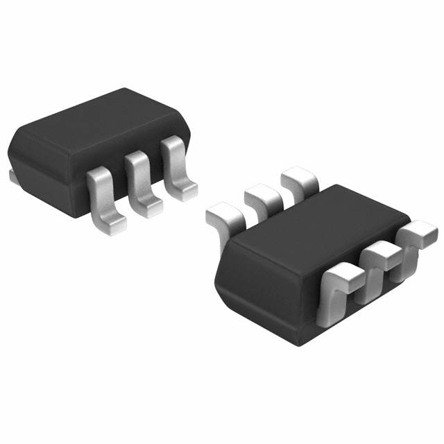
FDG316P P-Channel MOSFET Equivalent & Substitute Parts
Part Overview
The FDG316P is an active P-Channel MOSFET manufactured by onsemi, rated for 30V drain-to-source voltage and 1.6A continuous drain current. This device is housed in a 6-TSSOP (SC-88/SOT-363) surface mount package and is designed for low-power switching applications requiring compact form factors. The part is ROHS3 compliant with unlimited moisture sensitivity rating (MSL 1).
Substitute parts are identified when equivalent or superior electrical performance can be achieved within the same package footprint while maintaining compatibility with circuit design requirements and compliance standards.
Substiute Parts
Key Parameters
| Parameter | Value | Unit |
|---|---|---|
| FET Type | P-Channel | — |
| Drain-to-Source Voltage (Vdss) | 30 | V |
| Continuous Drain Current (Id) @ 25°C | 1.6 | A |
| On-Resistance (Rds On Max) @ Id, Vgs | 190 mOhm @ 1.6A, 10V | — |
| Gate Threshold Voltage (Vgs(th) Max) @ Id | 3 | V @ 250µA |
| Power Dissipation (Max) | 750 | mW |
| Operating Temperature Range | -55 to 150 | °C (TJ) |
| Package Type | 6-TSSOP (SC-88, SOT-363) | — |
| Mounting Type | Surface Mount | — |
| RoHS Status | ROHS3 Compliant | — |
Substitute Part Grouping Explanation
Substitution eligibility for the FDG316P is determined by the following critical parameters:
Package Compatibility: The substitute part must use the 6-TSSOP (SC-88/SOT-363) surface mount package to ensure PCB footprint compatibility without layout redesign.
FET Channel Type: The substitute must be P-Channel to maintain circuit polarity and gate drive requirements.
Voltage Rating: The substitute Vdss rating must be equal to or greater than 30V to support the same maximum operating voltage.
Current Rating: The substitute Id rating must be equal to or greater than 1.6A to handle the required continuous drain current without thermal derating.
Temperature Range: The substitute must support the operating temperature range of -55°C to 150°C (TJ).
Compliance: The substitute must maintain ROHS3 compliance and equivalent moisture sensitivity classification.
The NTJS4151PT1G meets these substitution criteria with identical package geometry, P-Channel configuration, and extended electrical performance characteristics.
Parameter Comparison
| Parameter | FDG316P | NTJS4151PT1G | Unit |
|---|---|---|---|
| Manufacturer | onsemi | onsemi | — |
| FET Type | P-Channel | P-Channel | — |
| Drain-to-Source Voltage (Vdss) | 30 | 20 | V |
| Continuous Drain Current (Id) @ 25°C | 1.6 | 3.3 | A |
| On-Resistance (Rds On Max) @ Rated Id, Vgs | 190 @ 1.6A, 10V | 60 @ 3.3A, 4.5V | mOhm |
| Gate Threshold Voltage (Vgs(th) Max) @ Id | 3 @ 250µA | 1.2 @ 250µA | V |
| Gate Charge (Qg Max) @ Vgs | 5 @ 10V | 10 @ 4.5V | nC |
| Input Capacitance (Ciss Max) @ Vds | 165 @ 15V | 850 @ 10V | pF |
| Power Dissipation (Max) | 750 | 1000 | mW |
| Gate Voltage (Vgs Max) | ±20 | ±12 | V |
| Operating Temperature Range | -55 to 150 | -55 to 150 | °C (TJ) |
| Package Type | 6-TSSOP (SC-88, SOT-363) | 6-TSSOP (SC-88, SOT-363) | — |
| Mounting Type | Surface Mount | Surface Mount | — |
| RoHS Status | ROHS3 Compliant | ROHS3 Compliant | — |
| Moisture Sensitivity Level (MSL) | 1 (Unlimited) | 1 (Unlimited) | — |
| Product Status | Active | Active | — |
Engineering Selection Recommendations
FDG316P Selection Criteria:
The FDG316P is appropriate for applications requiring a 30V voltage rating with moderate current handling (1.6A). This part supports higher gate voltage tolerance (±20V) and lower input capacitance (165 pF @ 15V), making it suitable for circuits with higher gate drive voltage margins or faster switching requirements with reduced capacitive loading.
NTJS4151PT1G Selection Criteria:
The NTJS4151PT1G is appropriate for applications where the circuit voltage does not exceed 20V and higher current capacity (3.3A) is beneficial. This part offers significantly lower on-resistance (60 mOhm vs. 190 mOhm), reduced gate threshold voltage (1.2V vs. 3V), and higher power dissipation capability (1W vs. 750mW). These characteristics result in lower conduction losses and improved thermal performance in current-limited applications.
Substitution Feasibility:
The NTJS4151PT1G cannot be used as a direct substitute for the FDG316P in circuits designed for 30V operation, as its 20V Vdss rating is insufficient. However, in applications where the actual operating voltage does not exceed 20V, the NTJS4151PT1G provides superior electrical performance with identical package compatibility and compliance certifications.
Both parts are active products from onsemi with ROHS3 compliance, unlimited moisture sensitivity rating (MSL 1), and identical operating temperature ranges (-55°C to 150°C TJ).
Frequently Asked Questions (FAQ)
Q: Can NTJS4151PT1G replace FDG316P in all applications?
A: No. The NTJS4151PT1G has a maximum Vdss rating of 20V, while the FDG316P is rated for 30V. Substitution is only valid in circuits where the actual drain-to-source voltage does not exceed 20V. Exceeding this voltage rating will cause device failure.
Q: What are the key performance differences between these parts?
A: The NTJS4151PT1G offers lower on-resistance (60 mOhm vs. 190 mOhm), lower gate threshold voltage (1.2V vs. 3V), higher continuous current rating (3.3A vs. 1.6A), and higher power dissipation capability (1W vs. 750mW). The FDG316P provides higher voltage rating (30V vs. 20V) and lower input capacitance (165 pF vs. 850 pF).
Q: Are the packages identical?
A: Yes. Both parts use the 6-TSSOP (SC-88/SOT-363) surface mount package with identical pinout and footprint. No PCB layout changes are required for physical substitution.
Q: Do both parts have the same compliance certifications?
A: Yes. Both the FDG316P and NTJS4151PT1G are ROHS3 compliant with MSL 1 (unlimited moisture sensitivity), REACH unaffected status, and EAR99 ECCN classification. Both are active products from onsemi.
Q: Which part should I select for a new design?
A: Select based on your circuit voltage requirements. If your design operates at or below 20V, the NTJS4151PT1G provides superior performance with lower losses and higher current capacity. If your design requires 30V operation or higher voltage margins, the FDG316P is the only suitable option.
Q: What is the impact of the lower gate threshold voltage in NTJS4151PT1G?
A: The lower Vgs(th) of 1.2V (vs. 3V) means the NTJS4151PT1G turns on at lower gate voltages, requiring less gate drive voltage and potentially reducing gate driver power consumption. This may require verification of gate drive circuit compatibility.
Q: How do the input capacitance differences affect circuit design?
A: The FDG316P has significantly lower input capacitance (165 pF vs. 850 pF). In high-frequency switching applications, lower capacitance reduces gate charge requirements and switching losses. The NTJS4151PT1G's higher capacitance may require stronger gate drive circuits at higher switching frequencies.
Alternative Parts

SJ6012L2TP
Littelfuse Inc.
6 Alternative Parts

JMK107BBJ476MA-RE
Taiyo Yuden
10 Alternative Parts

GMK107BBJ475MA-T
Taiyo Yuden
5 Alternative Parts
SJ6020N2ARP
Littelfuse Inc.
3 Alternative Parts
SJ6025R2ATP
Littelfuse Inc.
4 Alternative Parts

2474-05L
API Delevan Inc.
1 Alternative Parts

4590R-684K
API Delevan Inc.
1 Alternative Parts

CM6560R-334
API Delevan Inc.
1 Alternative Parts

CM6460-104
API Delevan Inc.
1 Alternative Parts

5526-12
API Delevan Inc.
1 Alternative Parts