


Request Quote
(Ships tomorrow)
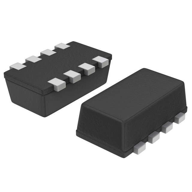
FDFMA2P857 Equivalent & Substitute Parts
Part Overview
The FDFMA2P857 is a P-Channel MOSFET manufactured by onsemi, rated for 20V drain-to-source voltage with 3A continuous drain current. This device features a PowerTrench® series design in a 6-MicroFET (2x2) surface mount package with an integrated Schottky diode. The part is classified as obsolete, necessitating identification of functionally equivalent alternatives for ongoing design support and procurement.
Substiute Parts
Key Parameters
| Parameter | Value |
|---|---|
| FET Type | P-Channel |
| Drain to Source Voltage (Vdss) | 20 V |
| Current - Continuous Drain (Id) @ 25°C | 3 A |
| Rds On (Max) @ Id, Vgs | 120 mOhm @ 3A, 4.5V |
| Vgs(th) (Max) @ Id | 1.3 V @ 250µA |
| Gate Charge (Qg) (Max) @ Vgs | 6 nC @ 4.5 V |
| Vgs (Max) | ±8 V |
| Input Capacitance (Ciss) (Max) @ Vds | 435 pF @ 10 V |
| Power Dissipation (Max) | 1.4 W |
| Operating Temperature Range | -55°C to 150°C |
| FET Feature | Schottky Diode (Isolated) |
| Mounting Type | Surface Mount |
| Package / Case | 6-VDFN Exposed Pad |
| Moisture Sensitivity Level (MSL) | 1 (Unlimited) |
Substitute Part Grouping Explanation
Substitution of the FDFMA2P857 is determined by strict electrical and mechanical parameter alignment within the P-Channel MOSFET category. The following parameters establish substitution eligibility:
Electrical Compatibility Criteria:
- FET Type: P-Channel (required match)
- Drain to Source Voltage (Vdss): 20 V (required match)
- Current - Continuous Drain (Id): Equal to or greater than 3 A
- Rds On (Max): Equal to or lower than 120 mOhm @ 4.5V
- Gate Charge (Qg): Comparable performance characteristics
- Vgs (Max): ±8 V (required match)
- Operating Temperature Range: -55°C to 150°C (required match)
- FET Feature: Schottky Diode (Isolated) (required match)
Mechanical Compatibility Criteria:
- Mounting Type: Surface Mount (required match)
- Moisture Sensitivity Level: MSL 1 or better
The NTHD3101FT1G meets these substitution criteria with equivalent electrical ratings and enhanced current capability (3.2A vs. 3A), lower on-resistance (80 mOhm vs. 120 mOhm), and identical voltage specifications.
Parameter Comparison
| Parameter | FDFMA2P857 | NTHD3101FT1G | Match Status |
|---|---|---|---|
| FET Type | P-Channel | P-Channel | Match |
| Drain to Source Voltage (Vdss) | 20 V | 20 V | Match |
| Current - Continuous Drain (Id) @ 25°C | 3 A | 3.2 A | Compatible (Higher) |
| Rds On (Max) @ Id, Vgs | 120 mOhm @ 3A, 4.5V | 80 mOhm @ 3.2A, 4.5V | Compatible (Lower) |
| Vgs(th) (Max) @ Id | 1.3 V @ 250µA | 1.5 V @ 250µA | Compatible |
| Gate Charge (Qg) (Max) @ Vgs | 6 nC @ 4.5 V | 7.4 nC @ 4.5 V | Compatible |
| Vgs (Max) | ±8 V | ±8 V | Match |
| Input Capacitance (Ciss) (Max) @ Vds | 435 pF @ 10 V | 680 pF @ 10 V | Compatible (Higher) |
| Power Dissipation (Max) | 1.4 W | 1.1 W | Compatible (Lower) |
| Operating Temperature Range | -55°C to 150°C | -55°C to 150°C | Match |
| FET Feature | Schottky Diode (Isolated) | Schottky Diode (Isolated) | Match |
| Mounting Type | Surface Mount | Surface Mount | Match |
| Moisture Sensitivity Level (MSL) | 1 (Unlimited) | 1 (Unlimited) | Match |
| REACH Status | REACH Unaffected | REACH Unaffected | Match |
| ECCN | EAR99 | EAR99 | Match |
Engineering Selection Recommendations
Both the FDFMA2P857 and NTHD3101FT1G are classified as obsolete products. The NTHD3101FT1G is the direct substitute for the FDFMA2P857 based on electrical and mechanical parameter equivalence.
Compliance and Certification Status:
- Both parts maintain REACH Unaffected status
- Both parts are classified under ECCN EAR99
- Both parts carry MSL 1 (Unlimited) moisture sensitivity rating
- NTHD3101FT1G includes RoHS3 Compliance certification
The NTHD3101FT1G provides superior electrical performance characteristics: higher continuous drain current (3.2A vs. 3A), lower on-resistance (80 mOhm vs. 120 mOhm), and lower maximum power dissipation (1.1W vs. 1.4W). These improvements result in reduced thermal stress and enhanced efficiency in switching applications.
Package differences exist: FDFMA2P857 uses 6-MicroFET (2x2) in 6-VDFN Exposed Pad configuration, while NTHD3101FT1G uses ChipFET™ in 8-SMD Flat Lead configuration. PCB layout and footprint modifications are required for substitution.
Frequently Asked Questions (FAQ)
Q: Can NTHD3101FT1G directly replace FDFMA2P857 without circuit modifications?
A: Electrical substitution is valid based on parameter compatibility. However, package differences (6-VDFN vs. 8-SMD) require PCB footprint redesign. Gate charge and input capacitance variations may affect switching speed characteristics in high-frequency applications.
Q: What are the key electrical advantages of NTHD3101FT1G over FDFMA2P857?
A: The NTHD3101FT1G provides 3.2A continuous drain current versus 3A, 80 mOhm on-resistance versus 120 mOhm, and 1.1W maximum power dissipation versus 1.4W. These parameters indicate improved thermal performance and reduced conduction losses.
Q: Are there package compatibility concerns?
A: Yes. FDFMA2P857 uses a 6-pin MicroFET package, while NTHD3101FT1G uses an 8-pin ChipFET package. Pin configurations differ, requiring complete PCB layout revision and schematic verification before implementation.
Q: Do both parts meet the same regulatory requirements?
A: Both parts are REACH Unaffected and classified as EAR99. NTHD3101FT1G includes RoHS3 Compliance certification, providing additional environmental compliance documentation. Both maintain MSL 1 moisture sensitivity rating.
Q: What is the impact of higher input capacitance in NTHD3101FT1G?
A: NTHD3101FT1G has 680 pF input capacitance versus 435 pF in FDFMA2P857. This higher capacitance may increase gate drive requirements and switching transition times in high-frequency switching circuits. Circuit simulation is necessary to evaluate impact on specific applications.
Q: Are both parts currently available for procurement?
A: Both parts are classified as obsolete. NTHD3101FT1G has higher inventory availability (29,100 pcs) compared to FDFMA2P857 (2,168 pcs), making it the preferred choice for new procurement activities.
Alternative Parts

SJ6012L2TP
Littelfuse Inc.
6 Alternative Parts

JMK107BBJ476MA-RE
Taiyo Yuden
10 Alternative Parts

GMK107BBJ475MA-T
Taiyo Yuden
5 Alternative Parts
SJ6020N2ARP
Littelfuse Inc.
3 Alternative Parts
SJ6025R2ATP
Littelfuse Inc.
4 Alternative Parts

2474-05L
API Delevan Inc.
1 Alternative Parts

4590R-684K
API Delevan Inc.
1 Alternative Parts

CM6560R-334
API Delevan Inc.
1 Alternative Parts

CM6460-104
API Delevan Inc.
1 Alternative Parts

5526-12
API Delevan Inc.
1 Alternative Parts